Datasheet4U Logo Datasheet4U.com

ABE0102 - (ABE0101 - ABE0106) Low EMI Spread Spectrum Multiplier Clock

Download the ABE0102 datasheet PDF. This datasheet also covers the ABE0101 variant, as both devices belong to the same (abe0101 - abe0106) low emi spread spectrum multiplier clock family and are provided as variant models within a single manufacturer datasheet.

General Description

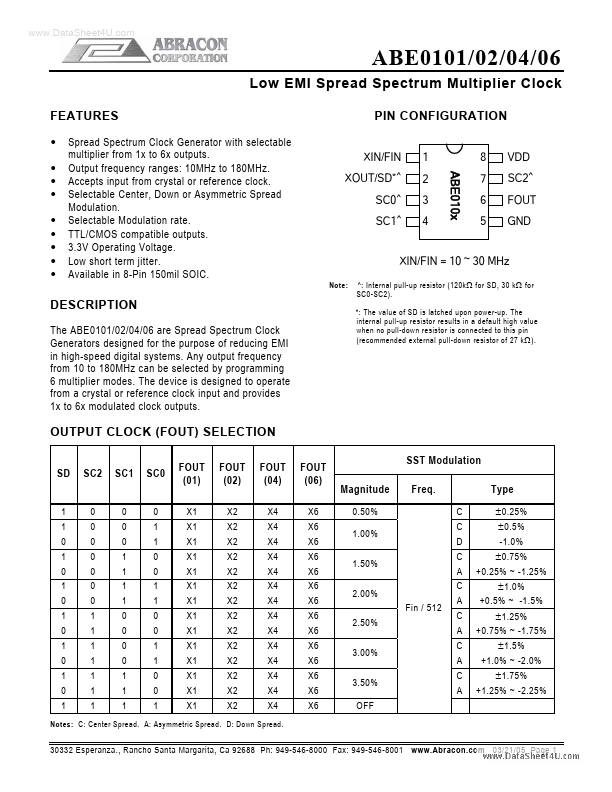
The ABE0101/02/04/06 are Spread Spectrum Clock Generators designed for the purpose of reducing EMI in high-speed digital systems.

Any output frequency from 10 to 180MHz can be selected by programming 6 multiplier modes.

Key Features

  • Spread Spectrum Clock Generator with selectable multiplier from 1x to 6x outputs. Output frequency ranges: 10MHz to 180MHz. Accepts input from crystal or reference clock. Selectable Center, Down or Asymmetric Spread Modulation. Selectable Modulation rate. TTL/CMOS compatible outputs. 3.3V Operating Voltage. Low short term jitter. Available in 8-Pin 150mil SOIC. PIN.

📥 Download Datasheet

Note: The manufacturer provides a single datasheet file (ABE0101_AbraconCorporation.pdf) that lists specifications for multiple related part numbers.

Datasheet Details

Part number ABE0102
Manufacturer Abracon Corporation
File Size 243.78 KB
Description (ABE0101 - ABE0106) Low EMI Spread Spectrum Multiplier Clock
Datasheet download datasheet ABE0102 Datasheet

Full PDF Text Transcription for ABE0102 (Reference)

Note: Below is a high-fidelity text extraction (approx. 800 characters) for ABE0102. For precise diagrams, tables, and layout, please refer to the original PDF.

www.DataSheet4U.com ABE0101/02/04/06 Low EMI Spread Spectrum Multiplier Clock FEATURES • • • • • • • • • Spread Spectrum Clock Generator with selectable multiplier from 1...

View more extracted text
• • Spread Spectrum Clock Generator with selectable multiplier from 1x to 6x outputs. Output frequency ranges: 10MHz to 180MHz. Accepts input from crystal or reference clock. Selectable Center, Down or Asymmetric Spread Modulation. Selectable Modulation rate. TTL/CMOS compatible outputs. 3.3V Operating Voltage. Low short term jitter. Available in 8-Pin 150mil SOIC. PIN CONFIGURATION XIN/FIN XOUT/SD*^ SC0^ SC1^ 1 8 VDD SC2^ FOUT GND ABE010x 2 3 4 7 6 5 XIN/FIN = 10 ~ 30 MHz Note: ^: Internal pull-up resistor (120k Ω for SD, 30 k Ω for SC0-SC2). *: The value of SD is latched upon power-up.