Datasheet Summary
v3.1
54SX Family FPGAs
Le a di ng E dg e P er f or m a nc e F ea t u r es
- 320 MHz Internal Performance
- 3.7 ns Clock-to-Out (Pin-to-Pin)
- 0.1 ns Input Set-Up
- 0.25 ns Clock Skew
Sp e ci f ic at ion s
- 66 MHz PCI
- CPLD and FPGA Integration
- Single Chip Solution
- 100% Resource Utilization with 100% Pin Locking
- 3.3V Operation with 5.0V Input Tolerance
- Very Low Power Consumption
- Deterministic, User-Controllable Timing
- Unique In-System Diagnostic and Debug capability with Silicon Explorer II
- Boundary Scan Testing in pliance with IEEE Standard 1149.1 (JTAG)
- Secure Programming Technology Prevents Reverse Engineering and Design Theft
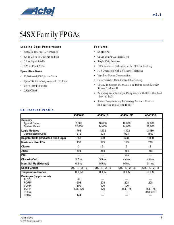
- 12,000 to 48,000 System Gates
- Up...