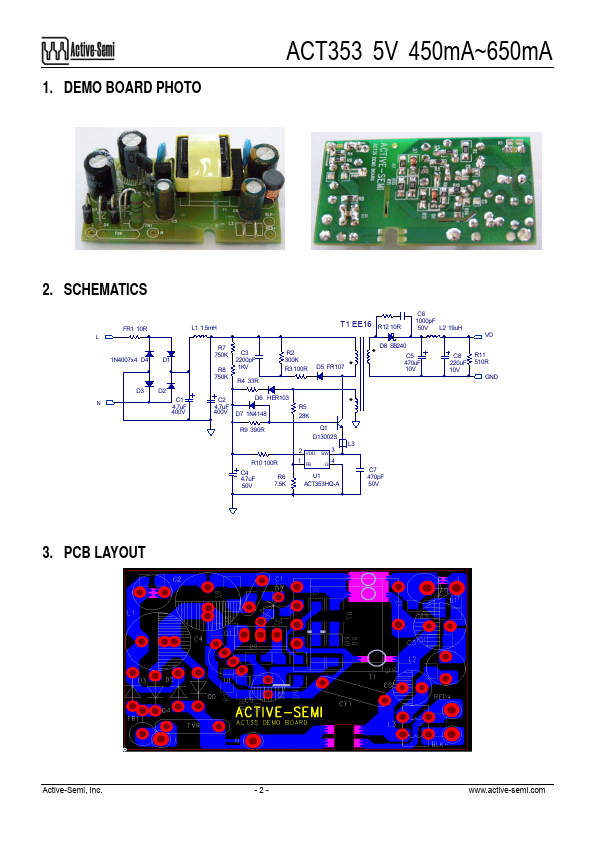
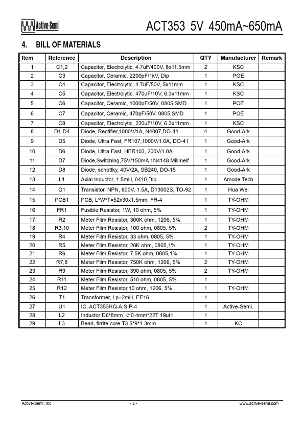
Active-Semi ACT353
Very Low Cost Cell Phone Charger
| Part No. | ACT353 |
|---|---|
| Datasheet | ACT353 Download |
| Manufacturer |  Active-Semi |
| Description | Very Low Cost Cell Phone Charger |
| Buy | Stock & Price |
FEATURES
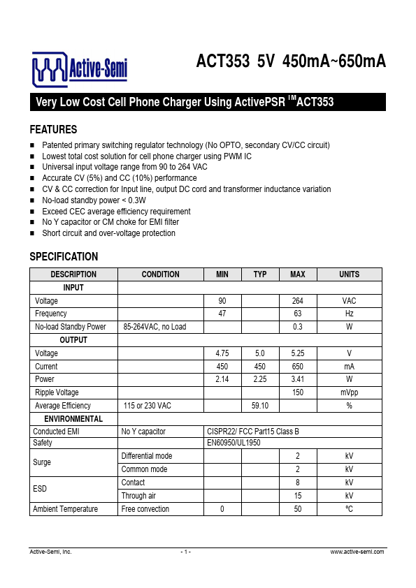
Patented primary switching regulator technology (No OPTO, secondary CV/CC circuit) Lowest total cost solution for cell phone charger using PWM IC Universal input voltage range from 90 to 264 VAC Accurate CV (5%) and CC (10%) performance CV & CC correction for Input line, output DC cord and transformer inductance variation No-load standby power < 0.3W Exceed CEC average efficiency requirement No Y capacitor or CM choke for EMI filter Short circuit and over-voltage protection SPECIFICATIONDESCRIPTION
INPUT Voltage Frequency No-load Standby Power OUTPUT Voltage Current Power Ripple Voltage Average Efficiency ENVIRONMENTAL Conducted EMI Safety Surge ESD Ambient Temperature CONDITION 85-264VAC, no Load 115 or 230 VAC No Y capacitor Differential mode Common mode Contact Through air Free convection MIN TYP MAX 90 264 47 63 0.3 4.75 5.0 5.25 450 450 650 2.14 2.25 3.41 150 59.10 CISPR22/ FCC Part15 Class B EN60950/UL1950 2 2 8 15 0 50 UNITS VAC Hz W V mA W mVpp % kV kV kV kV ºC Active-Semi, Inc. -1- 1.