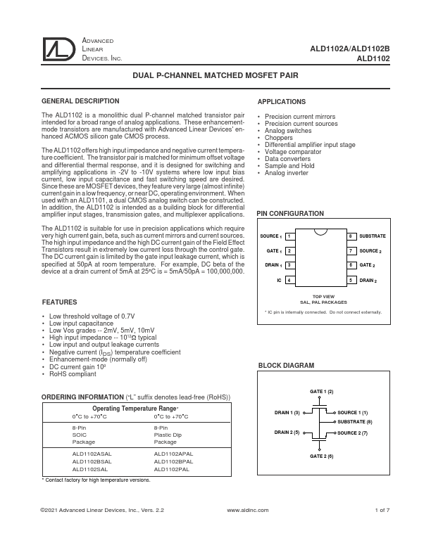
GENERAL DESCRIPTION
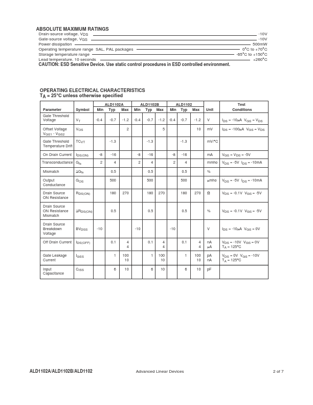
The transistor pair is matched for minimum offset voltage and differential thermal response, and it is designed for switching and amplifying applications in -2V to -10V systems where low input bias current, low input capacitance and fast switching speed are desired. Since these are MOSFET devices, they feature very large (almost infinite) current gain in a low frequency, or near DC, operating environment. When used with an ALD1101, a dual CMOS analog switch can be constructed. In addition, the ALD1102 is intended as a building block for differential amplifier input stages, transmission gates, and multiplexer applications. The ALD1102 is suitable for use in precision applications which require very high current gain, beta, such as current mirrors and current sources. The high input impedance and the high DC current gain of the Field Effect Transistors result in extremely low current loss through the control gate. The DC current gain is limited by the gate input leakage current, which is specified at 50pA at room temperature. Advanced Linear Devices