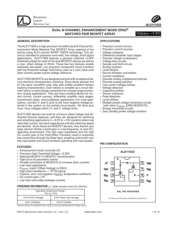
GENERAL DESCRIPTION
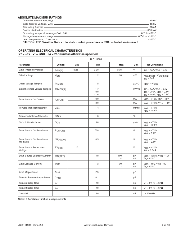
ALD111933 features a pecision matched +3.30V threshold voltage for each of the dual MOSFET devices as well as a max. offset voltage of 20mV. ALD111933 MOSFETs are designed and built with exceptional device electrical characteristics matching. Since these devices are on the same monolithic chip, they also exhibit excellent tempco tracking characteristics. Each device is versatile as a circuit element and is a useful design component for a broad range of precision analog applications. They are basic building blocks for current mirrors, current sources, differential amplifier input stages, transmission gates, and multiplexer applications. For most applications, connect V- and IC pins to the most negative voltage potential in the system on the printed circuit board. All other pins must have voltages within V+ and V- voltage limits. ALD111933 devices are built for minimum offset voltage and differential thermal response, and they are designed for switching and amplifying applications in +3.0V to +10V systems where low input bias current, low input capacitance and fast switching speed are desired. Advanced Linear Devices