GENERAL DESCRIPTION
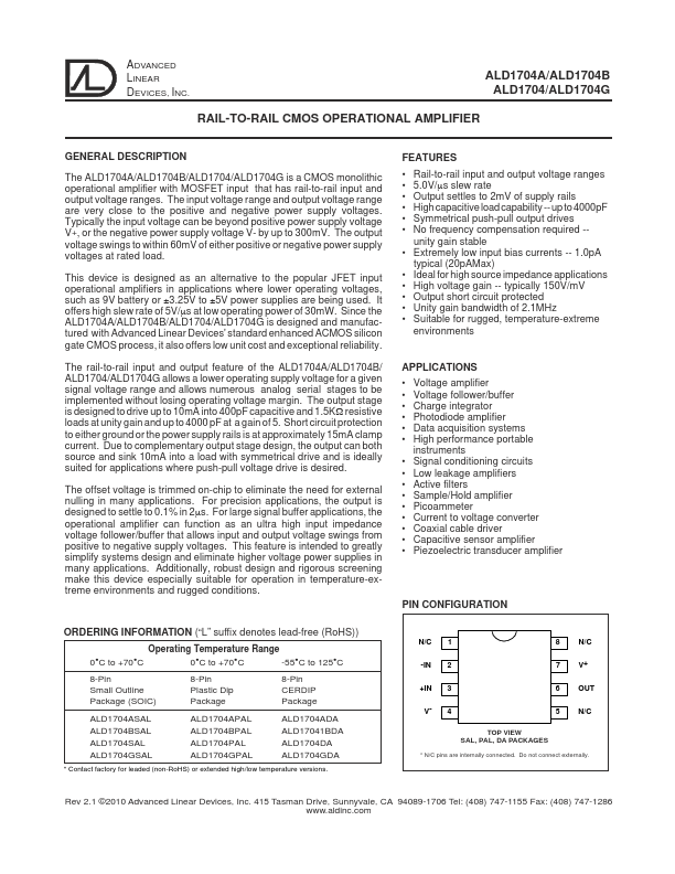
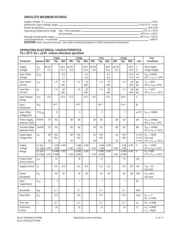
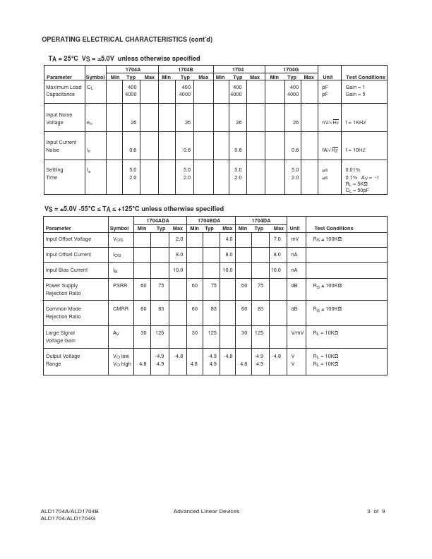
Typically the input voltage can be beyond positive power supply voltage V+, or the negative power supply voltage V- by up to 300mV. This device is designed as an alternative to the popular JFET input operational amplifiers in applications where lower operating voltages, such as 9V battery or ±3.25V to ±5V power supplies are being used. It offers high slew rate of 5V/µs at low operating power of 30mW. Since the ALD1704A/ALD1704B/ALD1704/ALD1704G is designed and manufactured with Advanced Linear Devices' standard enhanced ACMOS silicon gate CMOS process, it also offers low unit cost and exceptional reliability. The rail-to-rail input and output feature of the ALD1704A/ALD1704B/ ALD1704/ALD1704G allows a lower operating supply voltage for a given signal voltage range and allows numerous analog serial stages to be implemented without losing operating voltage margin. The output stage is designed to drive up to 10mA into 400pF capacitive and 1.5KΩ resistive loads at unity gain and up to 4000 pF at a gain of 5. Advanced Linear Devices