GENERAL DESCRIPTION
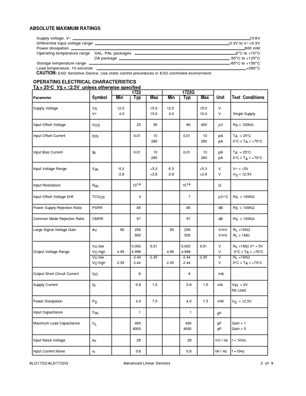
Input signal power is the product of input offset voltage and input bias current, which represents the minimum required power draw from the signal source in order to drive the input of the operational amplifier. Input signal power is also a figure of merit in source loading and its associated error, and is a measure of the basic signal resolution possible through the operational amplifier for a given signal source. The typical input loading at its input is 0.03 mV offset voltage and 0.01 pA input bias current at 25C, resulting in 0.0003 fW input signal power draw. This input characteristic virtually eliminates any loading effects on most types of signal sources, offering unparalled accuracy and signal integrity and fidelity. Obviously, for capacitive and high sensitivity, high impedance signal sources, the ALD1722/ALD1722G is ideally suited. It is readily suited for +5V single supply (or ±2V to ±5V) systems, with low operating power dissipation, a traditional strength of CMOS technology. Advanced Linear Devices