ALD2321A
ALD2321A is ULTRA LOW VOS EPAD DUAL CMOS ANALOG VOLTAGE COMPARATOR manufactured by Advanced Linear Devices.
- Part of the ALD2321 comparator family.
- Part of the ALD2321 comparator family.
DESCRIPTION
The ALD2321A/ALD2321B/ALD2321 is a monolithic Precision Dual Voltage parator, each having integrated dual plementary output drivers. It is constructed using advanced silicon gate CMOS technology. Key features of the ALD2321A/ALD2321B/ALD2321 include very high input impedance, very low offset voltage utilizing on-chip e-trim (EPAD® electronic-trimming) technology, flexible multiple output configurations and fast response time with small overdrive voltage. It is designed for ultra low level signal detection from high impedance sources. For many applications the ALD2321A/ALD2321B/ALD2321 can eliminate an input amplification stage, a precision input bias stage, a signal level shift stage and an output buffer stage, and do the entire job from low level input signal detection to high output driver -- all on a single chip.
The input voltage includes ground, making this voltage parator ideal for single supply (+5V) or dual supply (± 5V) powered systems. For dual supply applications, GND pin is connected to the most negative supply instead of Ground (0.0V). The negative supply voltage can be at any value between 0.0V and -5V. Each voltage parator is individually trimmed at the factory for minimum offset voltage at ground voltage potential, making the ALD2321A/ ALD2321B/ALD2321 at its best offset voltage and ready to pare very low signal level voltages at or near ground potential. Typically a signal less than 1m V can be resolved and detected reliably without requiring amplification. Sensor or detector signals with signal power as low as 0.004p W (4 x 10-15 Watt) can be readily detected.
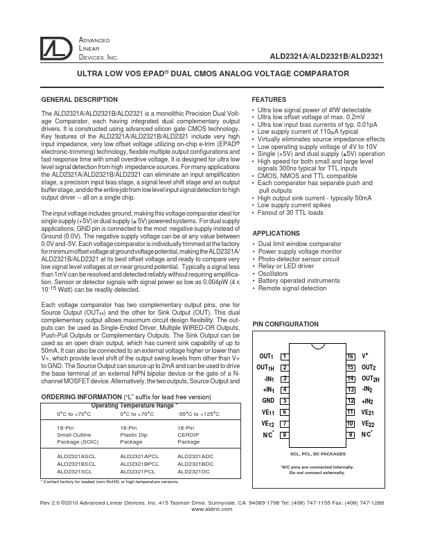
Each voltage parator has two plementary output pins, one for Source Output (OUTH) and the other for Sink Output (OUT). This dual plementary output allows maximum circuit design flexibility. The outputs can be used as Single-Ended Driver, Multiple WIRED-OR Outputs, Push-Pull Outputs or plementary Outputs. The Sink Output can be used as an open drain output, which has current sink...