GENERAL DESCRIPTION
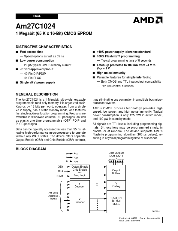
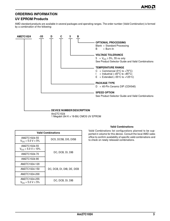
Products are available in windowed ceramic DIP packages, as well as plastic one time programmable (OTP) PDIP and PLCC packages. Data can be typically accessed in less than 55 ns, allowing high-performance microprocessors to operate without any WAIT states. AMD’s CMOS process technology provides high speed, low power, and high noise immunity. Typical power consumption is only 125 mW in active mode, and 100 µW in standby mode. All signals are TTL levels, including programming signals. Bit locations may be programmed singly, in blocks, or at random. The device supports AMD’s Flashrite programming algorithm (100 µs pulses), resulting in a typical programming time of 8 seconds. BLOCK DIAGRAM VCC VSS VPP OE# CE# PGM# Output Enable Chip Enable and Prog Logic Y Decoder A0–A15 Address Inputs Data Outputs DQ0–DQ15 Output Buffers Y Gating X Decoder 1,048,576 Bit Cell Matrix 06780J-1 Publication# 06780 Rev: J Amendment/0 Issue Date: May 1998 PRODUCT SELECTOR GUIDE Family Part N... Advanced Micro Devices