GENERAL DESCRIPTION
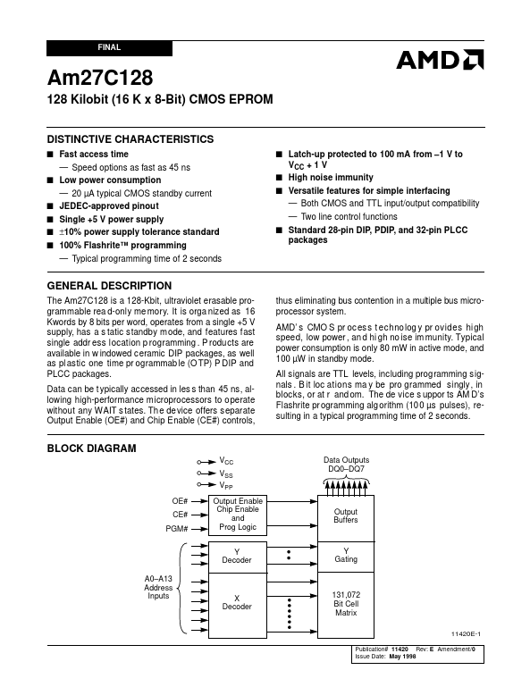
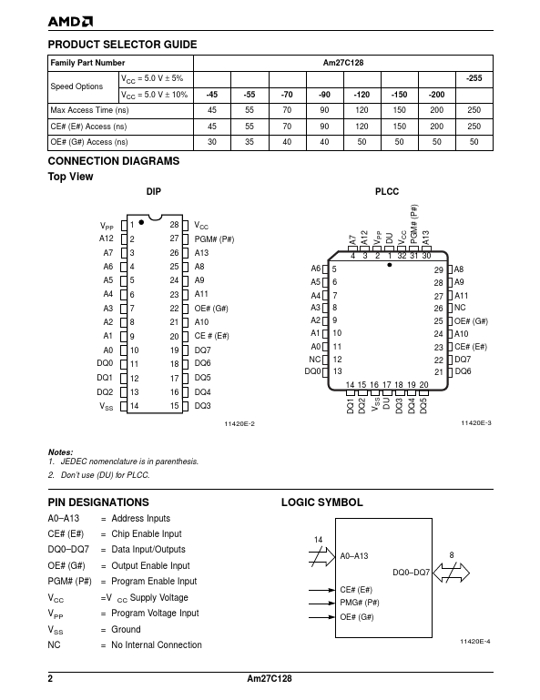
P roducts are available in w indowed ceramic DIP packages, as well as pl astic one time pr ogrammab le (O TP) P DIP and PLCC packages. Data can be t ypically accessed in les s than 45 ns, allowing high-performance microprocessors to operate without any WAIT s tates. Th e de vice offers separate Output Enable (OE#) and Chip Enable (CE#) controls, thus eliminating bus contention in a multiple bus microprocessor system. AMD’ s CMO S pr oc es s t echno log y pr ovides hi gh speed, low power , an d hi gh no ise im munity. Typical power consumption is only 80 mW in active mode, and 100 µW in standby mode. All signals are TTL levels, including prog ramming s ignals . B it loc ations ma y be pro grammed singly , in blocks, or at r and om. The de vice s uppor ts AM D’s Flashrite pr ogramming alg orithm (10 0 µs pulses), resulting in a typical programming time of 2 seconds. BLOCK DIAGRAM VCC VSS VPP OE# CE# PGM# Output Enable Chip Enable and Prog Logic Y Decoder A0–A13 Addres... Advanced Micro Devices