AP1802GU
AP1802GU is N-CHANNEL ENHANCEMENT MODE POWER MOSFET manufactured by Advanced Power Electronics Corp.
Pb Free Plating Product
Advanced Power Electronics Corp.
▼ Capable of 2.5V gate drive ▼ Lower on-resistance ▼ Surface mount package
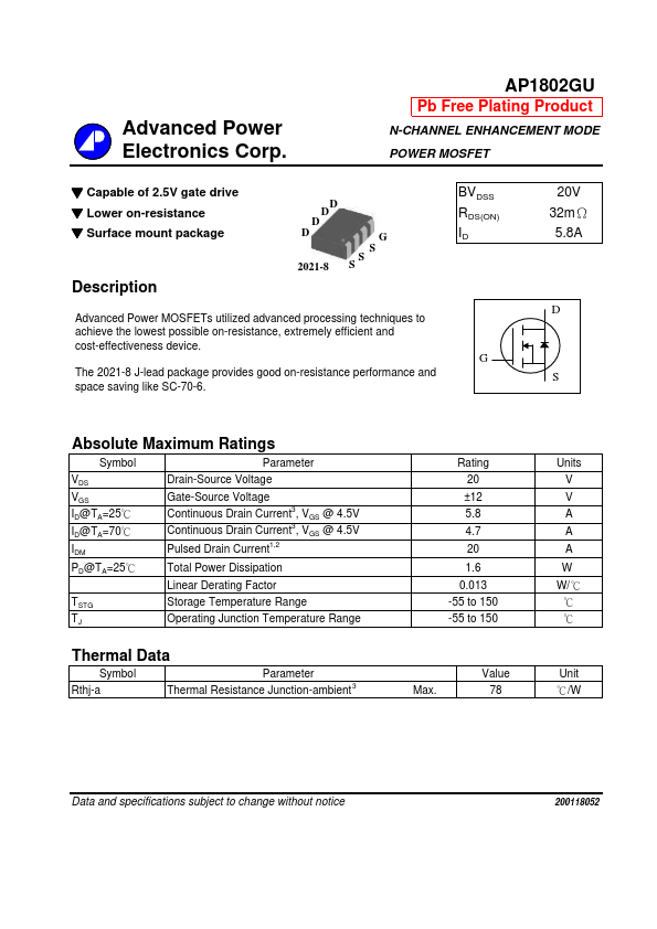
D 2021-8 S S S D D G D
N-CHANNEL ENHANCEMENT MODE POWER MOSFET
BVDSS RDS(ON) ID
20V 32mΩ 5.8A
Description
Advanced Power MOSFETs utilized advanced processing techniques to achieve the lowest possible on-resistance, extremely efficient and cost-effectiveness device.
The 2021-8 J-lead package provides good on-resistance performance and space saving like...