Datasheet4U Logo Datasheet4U.com

AP20T03GT-HF Datasheet N-channel Enhancement Mode Power MOSFET

Manufacturer: Advanced Power Electronics Corp

Overview: AP20T03GT-HF Halogen-Free Product Advanced Power Electronics Corp. ▼ Lower Gate Charge ▼ Simple Drive Requirement ▼ Fast Switching Characteristic ▼ RoHS pliant & Halogen-Free G N-CHANNEL ENHANCEMENT MODE POWER MOSFET D BVDSS RDS(ON) ID 30V 50mΩ 3.

General Description

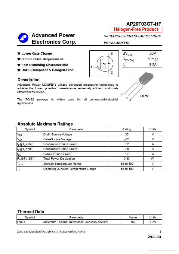
Advanced Power MOSFETs utilized advanced processing techniques to achieve the lowest possible on-resistance, extremely efficient and costeffectiveness device.

G The TO-92 applications.

package is widely used for all mercial-industrial D S TO-92 Absolute Maximum Ratings Symbol VDS VGS ID@TA=25℃ ID@TA=70℃ IDM PD@TA=25℃ TSTG TJ Parameter Drain-Source Voltage Gate-Source Voltage Continuous Drain Current Continuous Drain Current Pulsed Drain Current 1 Rating 30 +20 3.2 2.6 12 0.83 -55 to 150 -55 to 150 Units V V A A A W ℃ ℃ Total Power Dissipation Storage Temperature Range Operating Junction Temperature Range Thermal Data Symbol Rthj-a Parameter Maximum Thermal Resistance, Junction-ambient Value 150 Units ℃/W 1 201301081 Data and specifications subject to change without notice Free Datasheet http://../ AP20T03GT-HF Electrical Characteristics@Tj=25oC(unless otherwise specified) Symbol BVDSS RDS(ON) Parameter Drain-Source Breakdown Voltage Static Drain-Source On-Resistance2 Test Conditions VGS=0V, ID=250uA VGS=10V, ID=3A VGS=4.5V, ID=2A VGS(th) gfs IDSS IGSS Qg Qgs Qgd td(on) tr td(off) tf Ciss Coss Crss Rg Gate Threshold Voltage Forward Transconductance Drain-Source Leakage Current Gate-Source Leakage Total Gate Charge Gate-Source Charge Gate-Drain ("Miller") Charge Turn-on Delay Time Rise Time Turn-off Delay Time Fall Time Input Capacitance Output Capacitance Reverse Transfer Capacitance Gate Resistance VDS=VGS, ID=250uA VDS=5V, ID=3A VDS=24V, VGS=0V VGS= +20V, VDS=0V ID=3A VDS=15V VGS=4.5V VDS=15V ID=1A RG=3.3Ω VGS=10V VGS=0V VDS=25V f=1.0MHz f=1.0MHz Min.

AP20T03GT-HF Distributor