AP40T03J
AP40T03J is N-CHANNEL ENHANCEMENT MODE POWER MOSFET manufactured by Advanced Power Electronics Corp.
- Part of the AP40T03H comparator family.
- Part of the AP40T03H comparator family.
Description
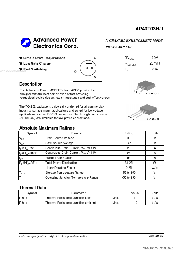
The Advanced Power MOSFETs from APEC provide the designer with the best bination of fast switching, ruggedized device design, low on-resistance and cost-effectiveness. The TO-252 package is universally preferred for all mercialindustrial surface mount applications and suited for low voltage applications such as DC/DC converters. The through-hole version (AP40T03J) are available for low-profile applications.
GD S
TO-252(H)
TO-251(J)
Absolute Maximum Ratings
Symbol VDS VGS ID@TA=25℃ ID@TA=100℃ IDM PD@TA=25℃ TSTG TJ Parameter Drain-Source Voltage Gate-Source Voltage Continuous Drain Current, VGS @ 10V Continuous Drain Current, VGS @ 10V Pulsed Drain Current
Rating 30 ±25 28 24 95 31.25 0.25 -55 to 150 -55 to 150
Units V V A A A W W/℃ ℃ ℃
Total Power Dissipation Linear Derating Factor Storage Temperature Range Operating Junction Temperature Range
Thermal Data
Symbol Rthj-c Rthj-a Parameter Thermal Resistance Junction-case Thermal Resistance Junction-ambient Max. Max. Value 4 110 Units ℃/W ℃/W
Data and specifications subject to change without notice
200331055-1/4
AP40T03H/J
Electrical Characteristics@Tj=25o C(unless otherwise specified)
Symbol BVDSS
ΔBVDSS/ΔTj
Parameter Drain-Source Breakdown Voltage
Test Conditions VGS=0V, ID=250u A
Min. 30 1
- Typ. 0.032
Max. Units 25 45 3 1 25 ±100 V V/℃ mΩ mΩ V S u A u A n A n C n C n C ns ns ns ns p F p F p F
Breakdown Voltage Temperature Coefficient Reference to 25℃, ID=1m A
RDS(ON)
..
Static Drain-Source On-Resistance
VGS=10V, ID=18A VGS=4.5V, ID=14A
15 8.8 2.5 5.8 6 62 16 4.4 655 145 95
VGS(th) gfs IDSS IGSS Qg Qgs Qgd td(on) tr td(off) tf Ciss Coss Crss
Gate Threshold Voltage Forward Transconductance
Drain-Source Leakage Current (T j=25 C) Drain-Source Leakage Current (T j=150 C) o o
VDS=VGS, ID=250u A VDS=10V, ID=18A VDS=30V, VGS=0V VDS=24V ,VGS=0V VGS= ±25V ID=18A VDS=20V VGS=4.5V VDS=15V ID=18A RG=3.3Ω,VGS=10V RD=0.83Ω VGS=0V VDS=25V f=1.0MHz
Gate-Source Leakage Total Gate Charge
Gate-Sour...