Datasheet Details
| Part number | APS04N60H-HF |
|---|---|
| Manufacturer | Advanced Power Electronics Corp |
| File Size | 77.62 KB |
| Description | N-CHANNEL ENHANCEMENT MODE POWER MOSFET |
| Datasheet | APS04N60H-HF_AdvancedPowerElectronics.pdf |
|
|
|
Overview: APS04N60H-HF Halogen-Free Product Advanced Power Electronics Corp. ▼ 100% Avalanche Test ▼ Fast Switching Characteristic ▼ Simple Drive Requirement ▼ RoHS pliant & Halogen-Free G S D N-CHANNEL ENHANCEMENT MODE POWER MOSFET BVDSS RDS(ON) ID 620V 2.
| Part number | APS04N60H-HF |
|---|---|
| Manufacturer | Advanced Power Electronics Corp |
| File Size | 77.62 KB |
| Description | N-CHANNEL ENHANCEMENT MODE POWER MOSFET |
| Datasheet | APS04N60H-HF_AdvancedPowerElectronics.pdf |
|
|
|
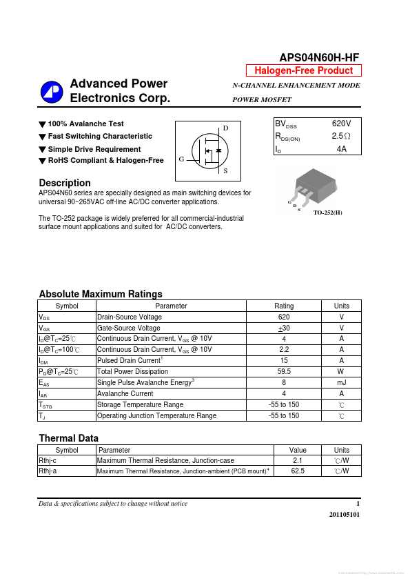
APS04N60 series are specially designed as main switching devices for universal 90~265VAC off-line AC/DC converter applications.
The TO-252 package is widely preferred for all mercial-industrial surface mount applications and suited for AC/DC converters.
G D S TO-252(H) Absolute Maximum Ratings Symbol VDS VGS ID@TC=25℃ ID@TC=100℃ IDM PD@TC=25℃ EAS IAR TSTG TJ Parameter Drain-Source Voltage Gate-Source Voltage Continuous Drain Current, V GS @ 10V Continuous Drain Current, V GS @ 10V Pulsed Drain Current 1 Rating 620 +30 4 2.2 15 59.5 3 Units V V A A A W mJ A ℃ ℃ Total Power Dissipation Single Pulse Avalanche Energy Avalanche Current Storage Temperature Range Operating Junction Temperature Range 8 4 -55 to 150 -55 to 150 Thermal Data Symbol Rthj-c Rthj-a Parameter Maximum Thermal Resistance, Junction-case Maximum Thermal Resistance, Junction-ambient (PCB mount) 4 Value 2.1 62.5 Units ℃/W ℃/W Data & specifications subject to change without notice 1 201105101 Free Datasheet http://../ APS04N60H-HF Electrical Characteristics@Tj=25 C(unless otherwise specified) Symbol BVDSS RDS(ON) VGS(th) gfs IDSS IGSS Qg Qgs Qgd td(on) tr td(off) tf Ciss Coss Crss Parameter Drain-Source Breakdown Voltage Static Drain-Source On-Resistance Gate Threshold Voltage Forward Transconductance Drain-Source Leakage Current Gate-Source Leakage Total Gate Charge 2 2 o Test Conditions VGS=0V, ID=250uA VGS=10V, ID=2A VDS=VGS, ID=250uA VDS=10V, ID=2A VDS=480V, VGS=0V VGS=+30V, VDS=0V ID=1A VDS=480V VGS=10V VDD=300V ID=2A RG=50Ω,VGS=10V RD=150Ω VGS=0V VDS=25V f=1.0MHz Min.
| Part Number | Description |
|---|---|
| APS8922A | 6A DUAL LOAD SWITCH |