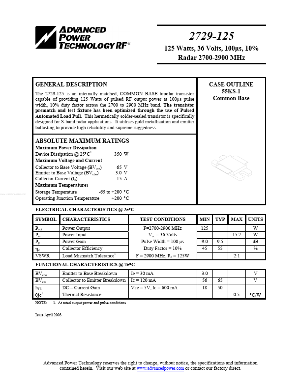
GENERAL DESCRIPTION
It utilizes gold metallization and emitter ballasting to provide high reliability and supreme ruggedness. CASE OUTLINE 55KS-1 Common Base ABSOLUTE MAXIMUM RATINGS
Maximum Power Dissipation 350 Device Dissipation @ 25°C1 Maximum Voltage and Current Collector to Base Voltage (BVces) 65 Emitter to Base Voltage (BVebo) 3.0 Collector Current (Ic) 15 Maximum Temperatures Storage Temperature -65 to +200 Operating Junction Temperature +200 W V V A °C °C ELECTRICAL CHARACTERISTICS
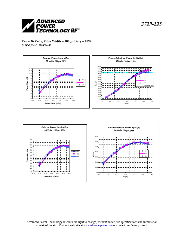
@ 25°C SYMBOL Pout Pin Pg ηc VSWR CHARACTERISTICS Power Output Power Input Power Gain Collector Efficiency Load Mismatch Tolerance1 TEST CONDITIONS F=2700-2900 MHz Vcc = 36 Volts Pulse Width = 100 µs Duty Factor = 10% F = 2900 MHz, Po = 125W Ie = 30 mA Ic = 120 mA Vce = 5V, Ic = 600 mA MIN 125 15.7 9.0 45 9.5 55 2:1 TYP MAX UNITS W W dB % FUNCTIONAL CHARACTERISTICS @ 25°C BVebo BVces hFE θjc1 NOTE: Emitter to Base Breakdown Collector to Emitter Breakdown DC – Current Gain Thermal Resistance 1. At r... Advanced Power Technology