DESCRIPTION
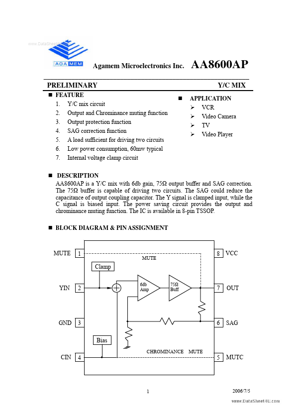
The Y signal is clamped input, while the C signal is biased input. The power saving circuit provides the output and chrominance muting function. The IC is available in 8-pin TSSOP. BLOCK DIAGRAM & PIN ASSIGNMENT MUTE 1 Clamp MUTE 8 VCC YIN 2 6db Amp 75Ω Buff 7 OUT GND 3 Bias 6 SAG CIN CHROMINANCE MUTE 4 5 MUTC 1 2006/7/5 Agamem Microelectronics Inc. ___________________________________________________________ PRELIMINARY Y/C MIX PIN DESCRIPTION
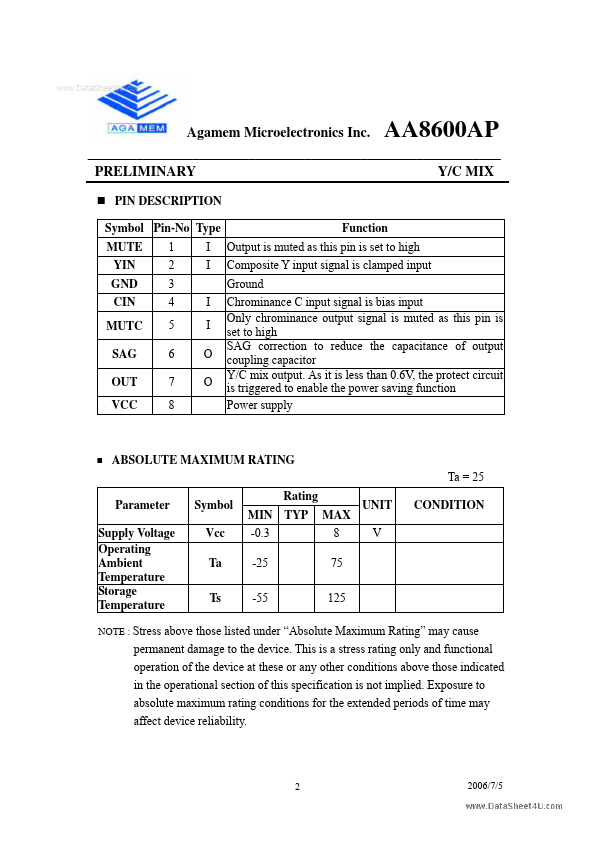
Symbol Pin-No Type MUTE YIN GND CIN MUTC SAG OUT VCC 1 2 3 4 5 6 7 8 I I O O I I Function Output is muted as this pin is set to high Composite Y input signal is clamped input Ground Chrominance C input signal is bias input Only chrominance output signal is muted as this pin is set to high SAG correction to reduce the capacitance of output coupling capacitor Y/C mix output. As it is less than 0.6V, the protect circuit is triggered to enable the power saving function Power supply AA8600AP ABSOLUTE MAXIMUM RATING Ta = 25 Parameter... Agamem Microelectronic