Overview: 
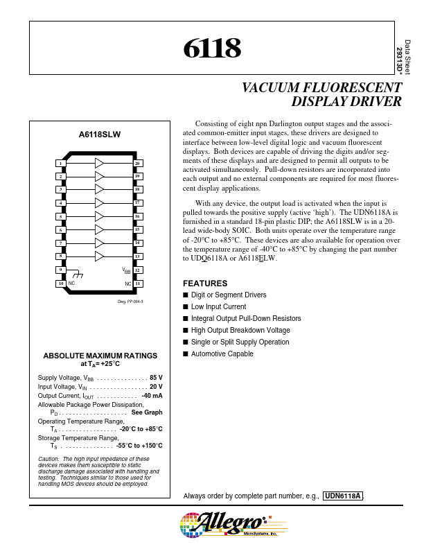
Data Sheet 29313D* 6118 A6118SLW 1 2 3 4 5 6 7 8 9 10 NC 20 19 18 17 16 15 14 13 VBB 12 NC 11
Dwg. PP-064-3 ABSOLUTE MAXIMUM RATINGS at TA= +25°C
Supply Voltage, VBB . . . . . . . . . . . . . . . 85 V Input Voltage, VIN . . . . . . . . . . . . . . . . . 20 V Output Current, IOUT . . . . . . . . . . . . -40 mA Allowable Package Power Dissipation,
PD . . . . . . . . . . . . . . . . . . . . See Graph Operating Temperature Range,
TA . . . . . . . . . . . . . . . . . -20°C to +85°C Storage Temperature Range,
TS . . . . . . . . . . . . . . . -55°C to +150°C
Caution: The high input impedance of these devices makes them susceptible to static discharge damage associated with handling and testing. Techniques similar to those used for handling MOS devices should be employed. VACUUM FLUORESCENT DISPLAY DRIVER
Consisting of eight npn Darlington output stages and the associated mon-emitter input stages, these drivers are designed to interface between low-level digital logic and vacuum fluorescent displays. Both devices are capable of driving the digits and/or segments of these displays and are designed to permit all outputs to be activated simultaneously. Pull-down resistors are incorporated into each output and no external ponents are required for most fluorescent display applications.
With any device, the output load is activated when the input is pulled towards the positive supply (active ‘high’). The UDN6118A is furnished in a standard 18-pin plastic DIP; the A6118SLW is in a 20lead wide-body SOIC. Both units operate over the temperature range of -20°C to +85°C. These devices are also available for operation over the temperature range of -40°C to +85°C by changing the part number to UDQ6118A or A6118ELW.