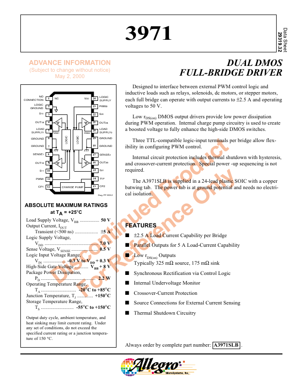
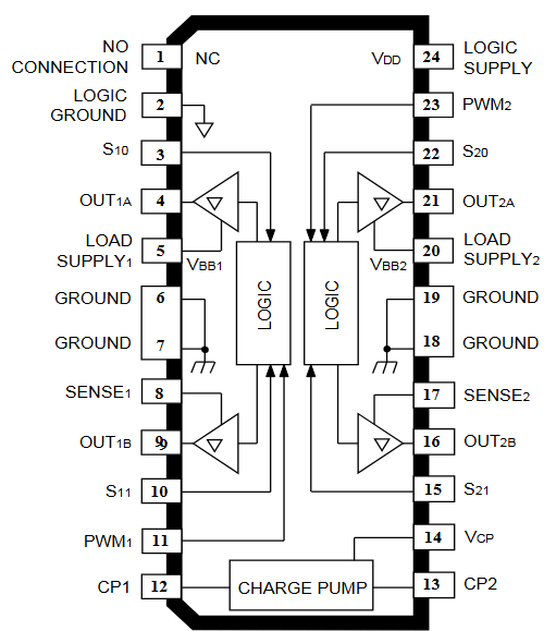
A3971 Overview
Key Specifications
Package: SOP
Operating Voltage: 5 V
Max Voltage (typical range): 5.5 V
Min Voltage (typical range): 4.5 V
Key Features
- s ±2.5 A Load Current Capability per Bridge s Parallel
Representative A3971 image (package may vary by manufacturer)