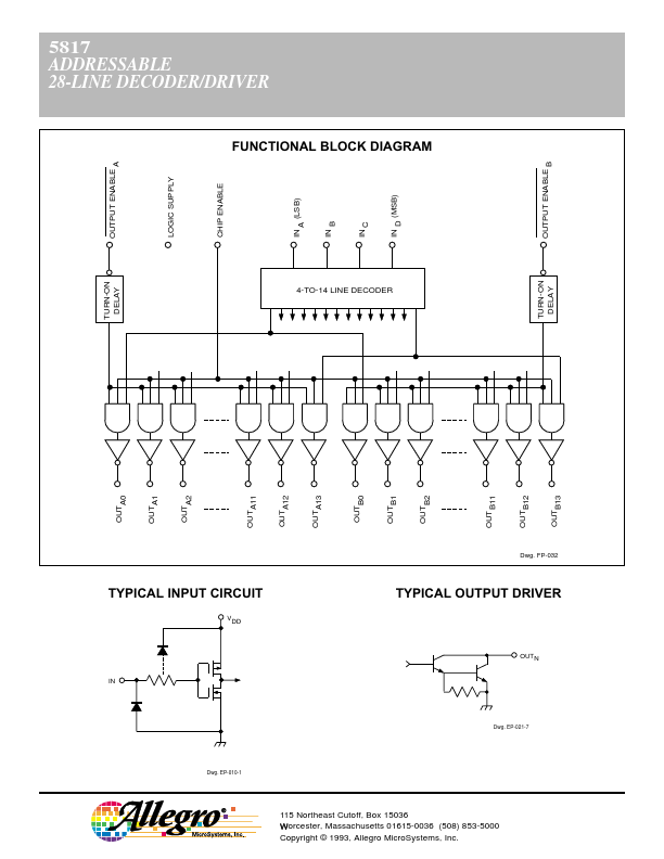
ABSOLUTE MAXIMUM RATINGS
at TA = 25°C Output Voltage, VCE ............................. 30 V Logic Supply Voltage, VDD .................. 7.0 V Input Voltage Range, VIN ....................... -0.3 V to VDD + 0.3 V Output Current, IC ........................... 600 mA Package Power Dissipation, PD ..... 2.70 W* Operating Temperature Range, TA ................................. -20°C to +85°C Storage Temperature Range, TS .............................. -55°C to +150°C *Derate at rate of 22 mW/°C above TA = 25°C. Caution: CMOS devices have input static protection but are susceptible to damage when exposed to extremely high static electrical charges. t y c l u n d O o . r e P P nc E d S e e 7 r u 1 e f 8 n i e 6 t R n A o r y c o b s F i D n ced w a o l h p S Re 39 38 37 36 35 34 33 32 31 OUTA0 OUTA1 OUTA2 OUTA3 OUTA4 OUTA5 OUTA6 OUTA7 OUTA8 OUTA9 GND OUTPUT DRIVER BANK B 4-TO-14 LINE DECODER OUTPUT DRIVER BANK A V DD 44 40 6 5 4 3 2 1 OUTPUT ENABLE A 30 29 25 19 20 18 21 22 23 24 OUTB11 OUTB10 OUTB13 OUTA11 A13 26 OUT B12 OUTA12 A10 IC IC 27 OUT OUT NC 28 Dwg. Allegro MicroSystems