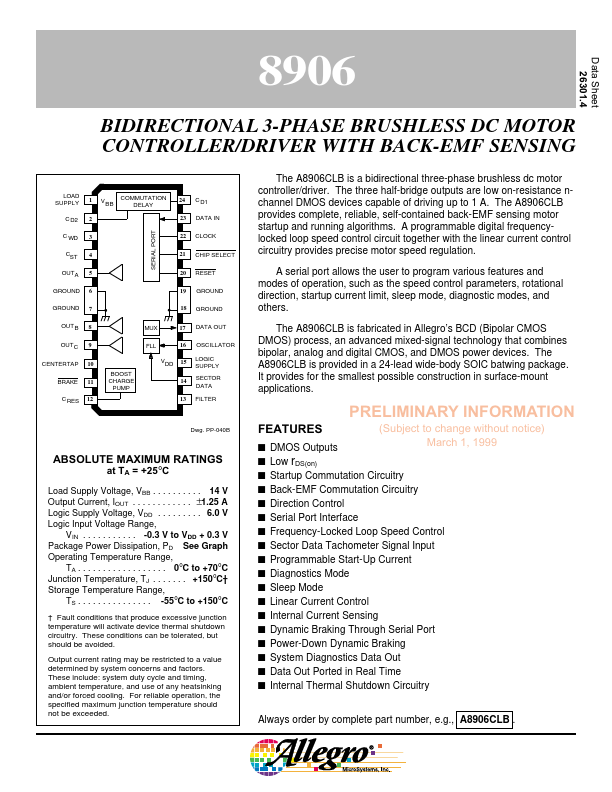
FEATURES
s s s s s s s s s s s s s s s s s s ABSOLUTE MAXIMUM RATINGS
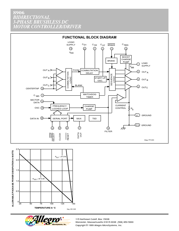
at TA = +25°C Load Supply Voltage, VBB . . . . . . . . . . 14 V Output Current, IOUT . . . . . . . . . . . . ±1.25 A Logic Supply Voltage, VDD . . . . . . . . . 6.0 V Logic Input Voltage Range, VIN . . . . . . . . . . . -0.3 V to VDD + 0.3 V Package Power Dissipation, PD See Graph Operating Temperature Range, TA . . . . . . . . . . . . . . . . . . 0°C to +70°C Junction Temperature, TJ . . . . . . . +150°C† Storage Temperature Range, TS . . . . . . . . . . . . . . . -55°C to +150°C † Fault conditions that produce excessive junction temperature will activate device thermal shutdown circuitry. These conditions can be tolerated, but should be avoided. Output current rating may be restricted to a value determined by system concerns and factors. These include: system duty cycle and timing, ambient temperature, and use of any heatsinking and/or forced cooling. For reliable operation, the specified maximum junction temperature should not be exceeded. Allegro MicroSystems