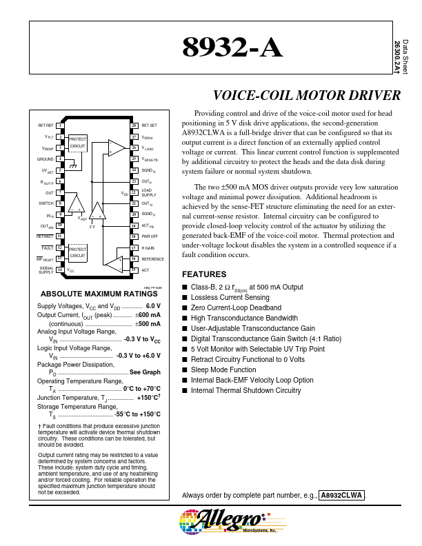
FEATURES
I I I I I I I I I I I Class-B, 2 Ω rDS(on) at 500 mA Output Lossless Current Sensing Zero Current-Loop Deadband High Transconductance Bandwidth User-Adjustable Transconductance Gain Digital Transconductance Gain Switch (4:1 Ratio) 5 Volt Monitor with Selectable UV Trip Point Retract Circuitry Functional to 0 Volts Sleep Mode Function Internal Back-EMF Velocity Loop Option Internal Thermal Shutdown Circuitry Dwg. PP-042B ABSOLUTE MAXIMUM RATINGS
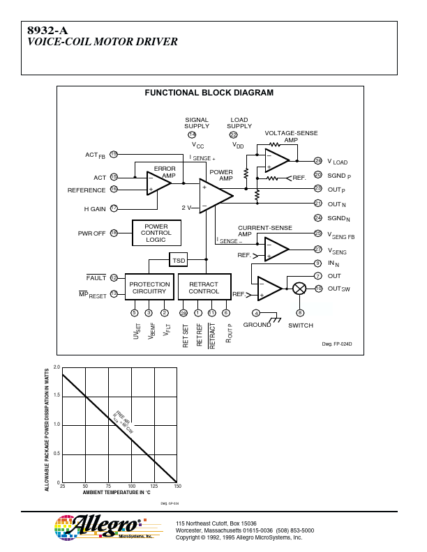
Supply Voltages, VCC and VDD ............ 6.0 V Output Current, IOUT (peak) ........... ±600 mA (continuous) ........................... ±500 mA Analog Input Voltage Range, VIN .................................... -0.3 V to VCC Logic Input Voltage Range, VIN ............................... -0.3 V to +6.0 V Package Power Dissipation, PD ......................................... See Graph Operating Temperature Range, TA ..................................... 0°C to +70°C Junction Temperature, TJ ............... +150°C† Storage Temperature... Allegro MicroSystems