ABSOLUTE MAXIMUM RATINGS
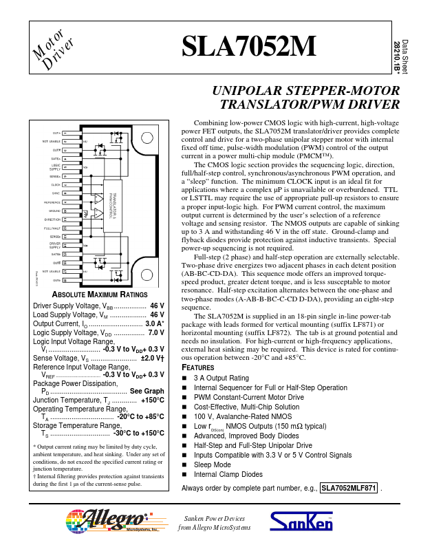
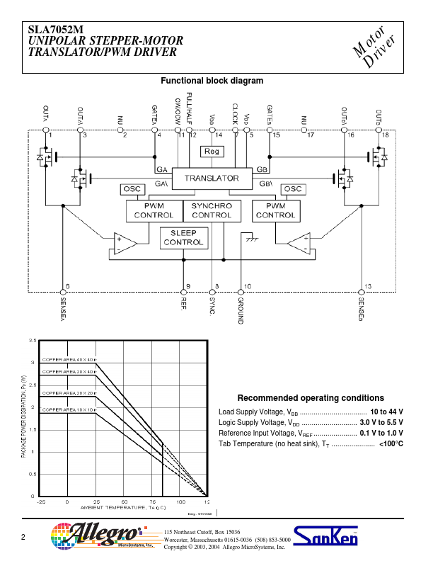
Driver Supply Voltage, VBB ................. 46 V Load Supply Voltage, VM ................... 46 V Output Current, IO ............................ 3.0 A* Logic Supply Voltage, VDD ................ 7.0 V Logic Input Voltage Range, VI ........................... -0.3 V to VDD+ 0.3 V Sense Voltage, VS ........................ ±2.0 V† Reference Input Voltage Range, VREF ................................... -0.3 V to VDD+ 0.3 V Package Power Dissipation, PD ........................................ See Graph Junction Temperature, TJ ............. +150°C Operating Temperature Range, TA ................................. -20°C to +85°C Storage Temperature Range, TS ............................... -30°C to +150°C * Output current rating may be limited by duty cycle, ambient temperature, and heat sinking. Under any set of conditions, do not exceed the specified current rating or junction temperature. † Internal filtering provides protection against transients during the first 1 µs of the current-sense pulse. Allegro MicroSystems