ABSOLUTE MAXIMUM RATINGS
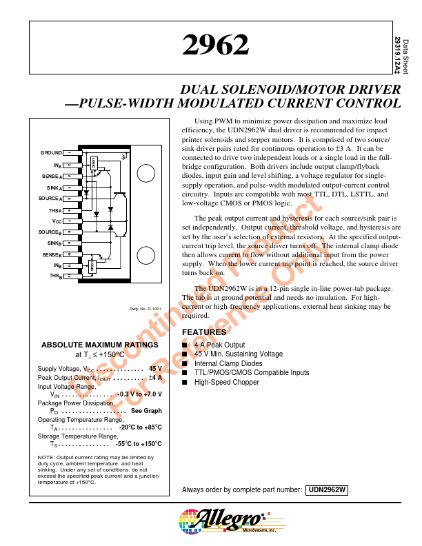
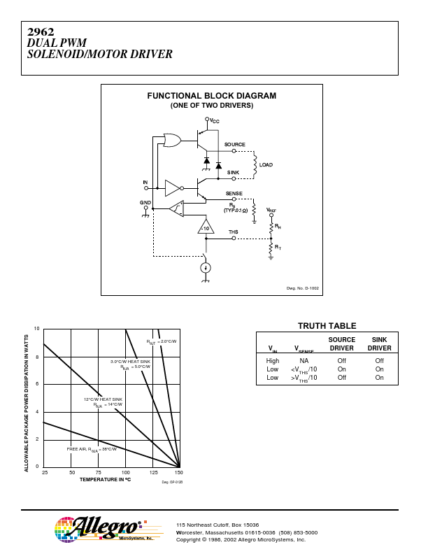
o fe at TJ ≤ +150°C Supply Voltage, VCC . . . . . . . . . . . . . . 45 V c e Peak Output Current, IOUT . . . . . . . . . ±4 A is R Input Voltage Range, VIN . . . . . . . . . . . . . . . -0.3 V to +7.0 V D r Package Power Dissipation, o PD . . . . . . . . . . . . . . . . . . . See Graph F Operating Temperature Range, supply operation, and pulse-width modulated output-current control circuitry. Inputs are compatible with most TTL, DTL, LSTTL, and low-voltage CMOS or PMOS logic. The peak output current and hysteresis for each source/sink pair is set independently. Output current, threshold voltage, and hysteresis are set by the user’s selection of external resistors. At the specified outputcurrent trip level, the source driver turns off. The internal clamp diode then allows current to flow without additional input from the power supply. When the lower current trip point is reached, the source driver turns back on. The UDN2962W is in a 12-pin single in-line power-tab package. Allegro MicroSystems