ASM3P2180A Overview
Description
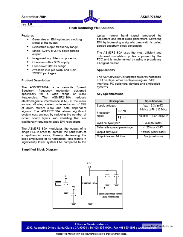
Supply voltages Frequency range FS1=0 FS1=1 Specification VDD = 3.3V ± 5% 6 MHz ≤ Fin ≤10 MHz 18 MHz ≤ Fin ≤ 30 MHz 325 pS (max) -1.25% or –2.4% 45/55% (worst case) 5ns (maximum) rev 1.0.
Key Features
- Generates an EMI optimized clocking signal at the output
- Selectable output frequency range
- Single 1.25% or 2.4% down spread output
- Integrated loop filter components
- Operates with a 3.3V supply
- Low-power CMOS design