AS7C164
AS7C164 is 5V 8K X 8 CMOS SRAM manufactured by Alliance Semiconductor.
2&72%(5#4<<<
®
$6:&497
89#;.[;#&026#65$0 )HDWXUHV
- AS7C164 (5V version)
- mercial temperatur
- Organization: 8,192 words × 8 bits
- Center power and ground pins
- High speed
- 12/15/20 ns address access time
- 3/4/5 ns output enable access time
- Low power consumption: ACTIVE
- 550 mW (AS7C164) / max @ 12 ns
- Low power consumption: STANDBY
- 11 mW (AS7C164) / max CMOS I/O
- 2.0V data retention
- Easy memory expansion with CE1, CE2, OE inputs
- TTL-patible, three-state I/O
- 28-pin JEDEC standard package
- 300 mil PDIP and SOJ
- ESD protection ≥ 2000 volts
- Latch-up current ≥ 200 mA
65$0
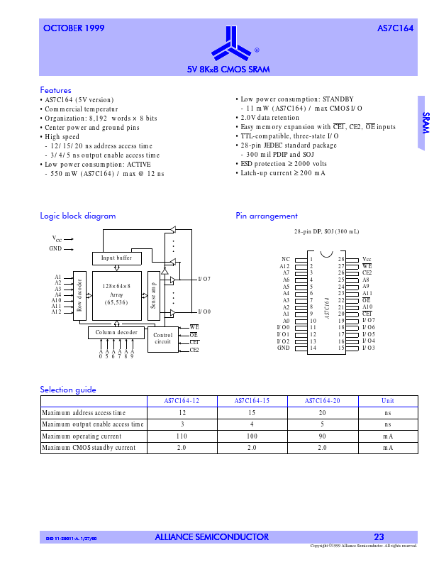
/RJLF#EORFN#GLDJUDP
VCC GND Input buffer A1 A2 A3 A4 A10 A11 A12 I/O7
3LQ#DUUDQJHPHQW
28-pin...