AS7C33128NTD36A
Overview
- Organization: 131,072 words × 32 or 36 bits NTD™1 architecture for efficient bus operation
- Fast clock speeds to 166 MHz in LVTTL/LVCMOS
- Fast clock to data access: 3.5/4.0/5.0 ns
- Fast OE access time: 3.5/4.0/5.0 ns
- Fully synchronous operation
- Flow-through or pipelined mode
- Asynchronous output enable control
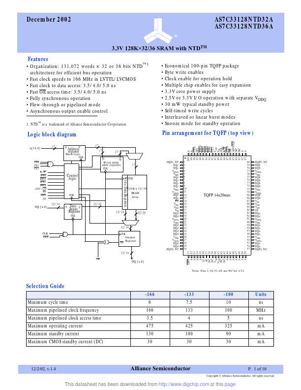
- NTD™ is a trademark of Alliance Semiconductor Corporation. Logic block diagram
- Economical 100-pin TQFP package
- Byte write enables