Datasheet Details
| Part number | AOD405 |
|---|---|
| Manufacturer | Alpha & Omega Semiconductors |
| File Size | 211.10 KB |
| Description | P-Channel MOSFET |
| Datasheet | AOD405_AlphaOmegaSemiconductors.pdf |
|
|
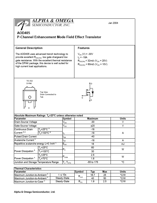
Overview: Jan 2004 AOD405 P-Channel Enhancement Mode Field Effect Transistor.
| Part number | AOD405 |
|---|---|
| Manufacturer | Alpha & Omega Semiconductors |
| File Size | 211.10 KB |
| Description | P-Channel MOSFET |
| Datasheet | AOD405_AlphaOmegaSemiconductors.pdf |
|
|
|
The AOD405 uses advanced trench technology to provide excellent RDS(ON), low gate chargeand low gate resistance.
With the excellent thermal resistance of the DPAK package, this device is well suited for high current load applications.
| Brand Logo | Part Number | Description | Manufacturer |
|---|---|---|---|
| AOD405 | P-Channel MOSFET | Freescale | |
| AOD405 | P-Channel 30V MOSFET | VBsemi |
| Part Number | Description |
|---|---|
| AOD400 | N-Channel MOSFET |
| AOD402 | N-Channel MOSFET |
| AOD403 | 30V P-Channel MOSFET |
| AOD404 | N-Channel MOSFET |
| AOD406 | N-Channel Enhancement Mode Field Effect Transistor |
| AOD407 | P-Channel MOSFET |
| AOD408 | N-Channel MOSFET |
| AOD409 | 60V P-Channel MOSFET |
| AOD409G | P-Channel MOSFET |
| AOD410 | N-Channel MOSFET |