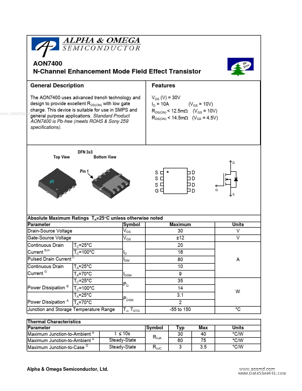
Datasheet4U Logo Datasheet4U.com

AON7400 - Field Effect Transistor

General Description

The AON7400 uses advanced trench technology and design to provide excellent R DS(ON) with low gate charge.

This device is suitable for use in SMPS and www.DataSheet4U.com general purpose applications.

Standard Product AON7400 is Pb-free (meets ROHS & Sony 259 specifications).

Key Features

  • VDS (V) = 30V (VGS = 10V) ID = 10A RDS(ON) < 12.5mΩ (VGS = 10V) RDS(ON) < 14.5mΩ (VGS = 4.5V) DFN 3x3 Top View Bottom View D Pin 1 S S S G D D D D G S Absolute Maximum Ratings TA=25°C unless otherwise noted Parameter Symbol VDS Drain-Source Voltage VGS Gate-Source Voltage Continuous Drain Current B,H Pulsed Drain Current Continuous Drain Current G Power Dissipation Power Dissipation B Maximum 30 ±12 20 16 80 10 9 35 14 3.1 2 -55 to 150 Units V V TC=25°C TC=100°C C ID IDM IDSM PD PDSM TJ.

📥 Download Datasheet

Full PDF Text Transcription (Reference)

The following content is an automatically extracted verbatim text from the original manufacturer datasheet and is provided for reference purposes only.

View original datasheet text
AON7400 N-Channel Enhancement Mode Field Effect Transistor General Description The AON7400 uses advanced trench technology and design to provide excellent R DS(ON) with low gate charge. This device is suitable for use in SMPS and www.DataSheet4U.com general purpose applications. Standard Product AON7400 is Pb-free (meets ROHS & Sony 259 specifications). Features VDS (V) = 30V (VGS = 10V) ID = 10A RDS(ON) < 12.5mΩ (VGS = 10V) RDS(ON) < 14.5mΩ (VGS = 4.5V) DFN 3x3 Top View Bottom View D Pin 1 S S S G D D D D G S Absolute Maximum Ratings TA=25°C unless otherwise noted Parameter Symbol VDS Drain-Source Voltage VGS Gate-Source Voltage Continuous Drain Current B,H Pulsed Drain Current Continuous Drain Current G Power Dissipation Power Dissipation B Maximum 30 ±12 20 16 80 10 9 35 14 3.