Datasheet Details
| Part number | AOTF470 |
|---|---|
| Manufacturer | Alpha & Omega Semiconductors |
| File Size | 69.56 KB |
| Description | N-Channel MOSFET |
| Datasheet |
 AOTF470 Datasheet AOTF470 Datasheet
|
|
|
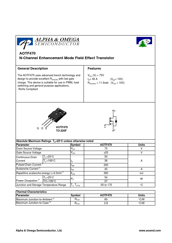
The AOTF470 uses advanced trench technology and design to provide excellent RDS(ON) with low gate charge.
This device is suitable for use in PWM, load switching and general purpose applications.
| Part number | AOTF470 |
|---|---|
| Manufacturer | Alpha & Omega Semiconductors |
| File Size | 69.56 KB |
| Description | N-Channel MOSFET |
| Datasheet |
AOTF470 Datasheet
|
|
|
|
| Part Number | Description | Manufacturer |
|---|---|---|
| AOTF474 | N-Channel MOSFET | INCHANGE |
| AOTF404 | N-Channel MOSFET | INCHANGE |
| AOTF409 | P-Channel MOSFET | INCHANGE |
| AOTF4126 | N-Channel MOSFET | INCHANGE |
| AOTF4185 | P-Channel MOSFET | INCHANGE |
| Part Number | Description |
|---|---|
| AOTF472 | 75V N-Channel MOSFET |
| AOTF474 | N-Channel MOSFET |
| AOTF409 | P-Channel MOSFET |
| AOTF4126 | N-Channel MOSFET |
| AOTF4185 | 40V P-Channel MOSFET |
The following content is an automatically extracted verbatim text from the original manufacturer datasheet and is provided for reference purposes only.