AOD403 Overview
Key Specifications
Package: DPAK
Mount Type: Surface Mount
Pins: 3
Max Operating Temp: 175 °C
Description
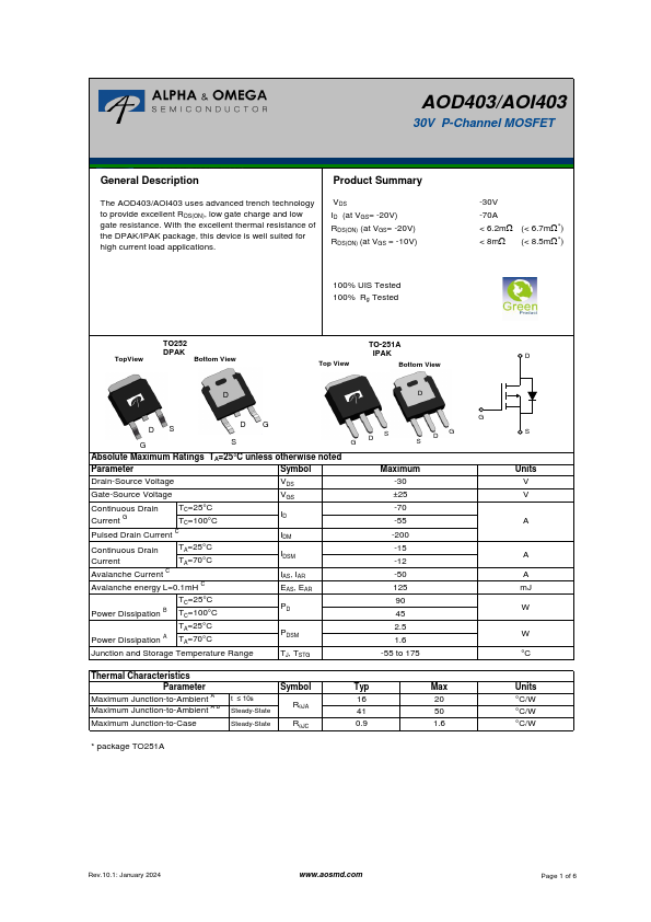
Product Summary The AOD403/AOI403 uses advanced trench technology to provide excellent RDS(ON), low gate charge and low gate resistance. With the excellent VDS ID (at VGS= -20V) RDS(ON) (at VGS= -20V) RDS(ON) (at VGS = -10V) 100% UIS Tested 100% Rg Tested -30V -70A < 6.2mW < 8mW (< 6.7mW*) (< 8.5mW*) TopView TO252 DPAK Bottom View Top View TO-251A IPAK Bottom View D D DS G DG S G DS G G SD Parameter Symbol Maximum Drain-Source Voltage VDS -30 Gate-Source Voltage VGS ±25 Continuous Drain Current G TC=25°C TC=100°C ID Pulsed Drain Current C IDM -70 -55 -200 Continuous Drain Current TA=25°C TA=70°C IDSM -15 -12 Avalanche Current C IAS, IAR -50 Avalanche energy L=0.1mH C EAS, EAR 125 TC=25°C Power Dissipation B TC=100°C PD 90 45 TA=25°C Power Dissipation A TA=70°C PDSM 2.5 1.6 Junction and Storage Temperature Range TJ, TSTG -55 to 175 Parameter Symbol Typ Maximum Junction-to-Ambient A t ≤ 10s Maximum Junction-to-Ambient A D Steady-State RqJA 16 41 Maximum Junction-to-Case Steady-State RqJC 0.9 Max 20 50 1.6 * package TO251A D S Units V V A A A mJ W W °C Units °C/W °C/W °C/W Rev.10.1: January 2024 Page 1 of 6 AOD403/AOI403 Symbol Parameter STATIC PARAMETERS BVDSS Drain-Source Breakdown Voltage IDSS Zero Gate Voltage Drain Current IGSS VGS(th) ID(ON) Gate-Body leakage current Gate Threshold Voltage On state drain current RDS(ON) Static Drain-Source On-Resistance Conditions Min Typ Max Units ID=-250mA, VGS=0V -30 V VDS=-30V, VGS=0V TJ=55°C -1 mA -5 VDS=0V, VGS= ±25V ±100 nA VDS=VGS ID=-250mA -1.5 -2.5 -3.5 V VGS=-10V, VDS=-5V -200 A VGS=-20V, ID=-2.