AOE6930 Overview
Key Specifications
Max Operating Temp: 150 °C
Min Operating Temp: -55 °C
Description
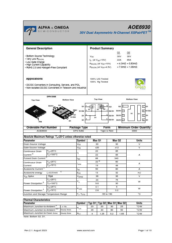
Bottom Source Technology - Very Low RDS(ON) - Low Gate Charge - High Current Capability - RoHS 2.0 and Halogen-Free Compliant Product Summary VDS ID (at VGS=10V) RDS(ON) (at VGS=10V) RDS(ON) (at VGS=4.5V) Q1 Q2 30V 30V 22A 85A < 4.3mΩ < 0.83mΩ < 7.0mΩ < 1.05mΩ.