AON4701
AON4701 is Field Effect Transistor manufactured by Alpha & Omega Semiconductors.
Description
The AON4701 uses advanced trench technology to provide excellent R DS(ON) and low gate charge. A Schottky diode is provided to facilitate the implementation .. of a bidirectional blocking switch, or for DC-DC conversion applications. Standard Product AON4701 is Pb-free (meets ROHS & Sony 259 specifications). AON4701L is a Green Product ordering option. AON4701 and AON4701L are electrically identical.
Features
VDS (V) = -20V ID = -3.4A (VGS = -4.5V) RDS(ON) < 90mΩ (VGS = -4.5V) RDS(ON) < 120mΩ (VGS = -2.5V) RDS(ON) < 160mΩ (VGS = -1.8V) SCHOTTKY VDS (V) = 20V, IF = 1A, VF<0.5V@0.5A
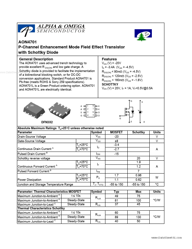
D A A S G 1 2 3 4 8 7 6 5 K K D D G S
DFN3X2 Absolute Maximum Ratings TA=25°C unless otherwise noted Symbol Parameter VDS Drain-Source Voltage V Gate-Source Voltage GS TA=25°C ID Continuous Drain Current A TA=70°C IDM Pulsed Drain Current B VKA Schottky reverse voltage TA=25°C IF A Continuous Forward Current TA=70°C IFM Pulsed Forward Current B TA=25°C PD TA=70°C Power Dissipation TJ, TSTG Junction and Storage Temperature Range Parameter: Thermal Characteristics MOSFET t ≤ 10s Maximum Junction-to-Ambient A A Steady-State Maximum Junction-to-Ambient Steady-State Maximum Junction-to-Lead C Thermal Characteristics Schottky t ≤ 10s Maximum Junction-to-Ambient A A Steady-State Maximum Junction-to-Ambient C Steady-State Maximum Junction-to-Lead Symbol RθJA RθJL RθJA RθJL MOSFET -20 ±8 -3.4 -2.7 -15
Schottky
Units V V A
20 1.9 1.2 1.7 1.1 -55 to 150 Typ 49 81 37 60 89 40 7 0.96 0.62 -55 to 150 Max 75 100 45 75 130 50
W °C Units °C/W
°C/W
Electrical Characteristics (T J=25°C unless otherwise noted) Parameter Symbol STATIC PARAMETERS BVDSS Drain-Source Breakdown Voltage IDSS IGSS VGS(th) ID(ON) RDS(ON) .. g FS VSD IS Zero Gate Voltage Drain Current Gate-Body leakage current Gate Threshold Voltage On state drain current Conditions ID=-250µA, VGS=0V VDS=-16V, VGS=0V TJ=55°C VDS=0V, VGS=±8V VDS=VGS ID=-250µA VGS=-4.5V, VDS=-5V VGS=-4.5V, ID=-3.4A TJ=125°C -0.3...