AONV310A60 Overview
Description
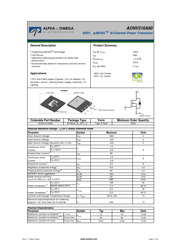
Proprietary aMOS5TM technology - Low RDS(ON) - Optimized switching parameters for better EMI performance - Enhanced body diode for robustness and fast reverse recovery.
| Part | AONV310A60 |
|---|---|
| Description | N-Channel Power Transistor |
| Category | Transistor |
| Manufacturer | Alpha & Omega Semiconductors |
| Size | 485.43 KB |
Proprietary aMOS5TM technology - Low RDS(ON) - Optimized switching parameters for better EMI performance - Enhanced body diode for robustness and fast reverse recovery.
| Part Number | Manufacturer | Description |
|---|---|---|
| BDT88 | Inchange Semiconductor | Silicon PNP Power Transistor |
| KD333 | Tesla Elektronicke | Transistor |
| C828 | SEMTECH | NPN Silicon Transistor |