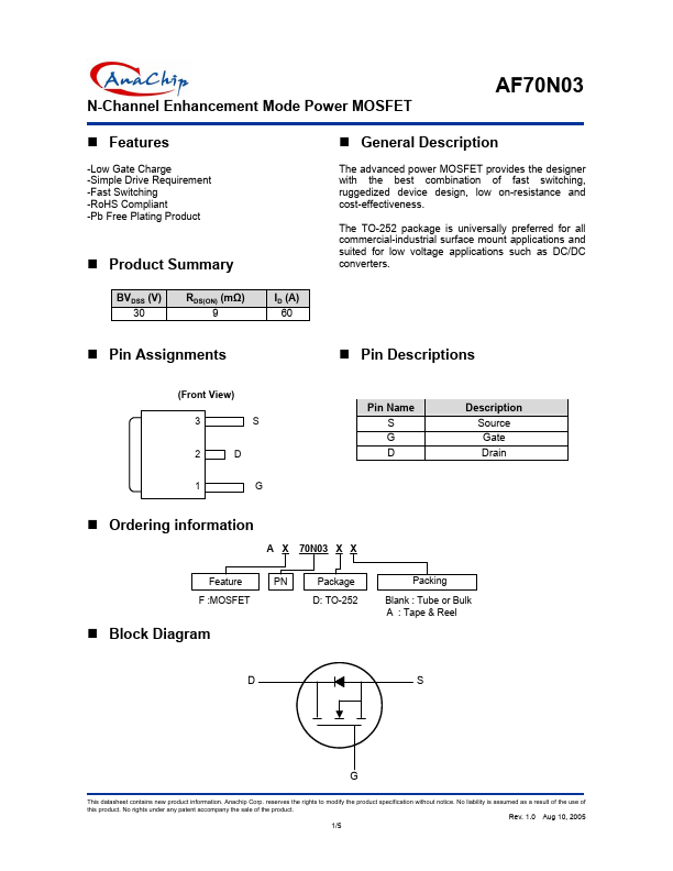
FEATURES
-Low Gate Charge -Simple Drive Requirement -Fast Switching -RoHS Compliant -Pb Free Plating Product Product Summary GENERAL DESCRIPTION
BVDSS (V) 30 RDS(ON) (mΩ) 9 ID (A) 60 Pin Assignments Pin Descriptions (Front View) 3S 2D 1G Pin Name S G D DESCRIPTION
Source Gate Drain Ordering information A X 70N03 X X Feature PN Package F :MOSFET D: TO-252 Block Diagram Packing Blank : Tube or Bulk A : Tape & Reel DS G This datasheet contains new product information. Anachip Corp. reserves the rights to modify the product specification without notice. No liability is assumed as a result of the use of this product. No rights under any patent accompany the sale of the product. Rev. 1.0 Aug 10, 2005 1/5 N-Channel Enhancement Mode Power MOSFET AF70N03 ABSOLUTE MAXIMUM RATINGS
Symbol VDS VGS Drain-Source Voltage Gate-Source Voltage Parameter ID Continuous Drain Current, VGS=10V IDM PD TSTG TJ Pulsed Drain Current (Note 1) Total Power Dissipation Linear Derating Factor Storage Te... Anachip