420AR-32 Overview
Key Specifications
Package: SOIC W
Pins: 24
Max Voltage (typical range): 32 V
Min Voltage (typical range): 12 V
Key Features
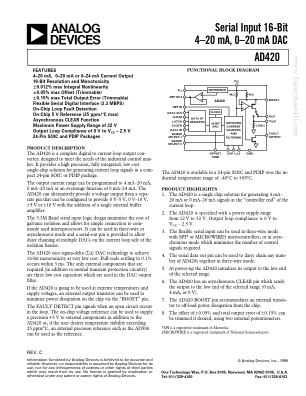
- 24 mA Current Output 16-Bit Resolution and Monotonicity ؎ 0.012% max Integral Nonlinearity ؎ 0.05% max Offset (Trimmable) ؎ 0.15% max Total Output Error (Trimmable) Flexible Serial Digital Interface (3.3 MBPS) On-Chip Loop Fault Detection On-Chip 5 V Reference (25 ppm/؇C max) Asynchronous CLEAR Function Maximum Power Supply Range of 32 V Output Loop Compliance of 0 V to VCC
- 2.5 V 24-Pin SOIC and PDIP Packages PRODUCT DESCRIPTION