FEATURES
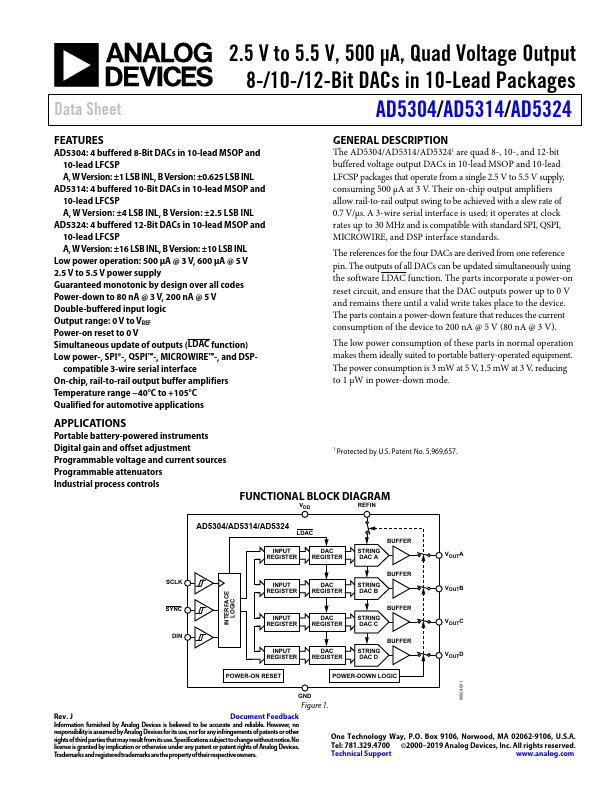
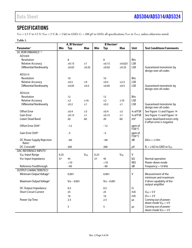
AD5304: 4 buffered 8-Bit DACs in 10-lead MSOP and 10-lead LFCSP A, W Version: ±1 LSB INL, B Version: ±0.625 LSB INL AD5314: 4 buffered 10-Bit DACs in 10-lead MSOP and 10-lead LFCSP A, W Version: ±4 LSB INL, B Version: ±2.5 LSB INL AD5324: 4 buffered 12-Bit DACs in 10-lead MSOP and 10-lead LFCSP A, W Version: ±16 LSB INL, B Version: ±10 LSB INL Low power operation: 500 μA @ 3 V, 600 μA @ 5 V 2.5 V to 5.5 V power supply Guaranteed monotonic by design over all codes Power-down to 80 nA @ 3 V, 200 nA @ 5 V Double-buffered input logic Output range: 0 V to VREF Power-on reset to 0 V Simultaneous update of outputs (LDAC function) Low power-, SPI®-, QSPI™-, MICROWIRE™-, and DSP- compatible 3-wire serial interface On-chip, rail-to-rail output buffer amplifiers Temperature range −40°C to +105°C Qualified for automotive applications GENERAL DESCRIPTION
Their on-chip output amplifiers allow rail-to-rail output swing to be achieved with a slew rate of 0.7 V/μs. A 3-wire serial interface is used; it operates at clock rates up to 30 MHz and is compatible with standard SPI, QSPI, MICROWIRE, and DSP interface standards. Analog Devices