AD5583
AD5583 is 12-/10-Bit Digital-to-Analog Converter manufactured by Analog Devices.
Data Sheet AD5582/AD5583
Quad, Parallel Input, Voltage Output, 12-/10-Bit Digital-to-Analog Converter
Features
- 12-bit linearity and monotonic AD5582
- 10-bit linearity and monotonic AD5583
- Wide operating range: single 5 V to 15 V or dual ±5 V supply
- Unipolar or bipolar operation
- Double buffered registers enable independent or simultaneous multichannel updates
- 4 independent rail-to-rail reference inputs
- 20 m A high current output drive
- Parallel interface
- Data readback capability
- 5 µs settling time
- Built-in matching resistor simplifies negative reference
- Unconditionally stable under any capacitive loading
- pact footprint: TSSOP-48
- Extended temperature range:
- 40°C to +125°C
APPLICATIONS
- Process control equipment
- Closed-loop servo control
- Data acquisition systems
- Digitally controlled calibration
- Optical network control loops
- 4 m A to 20 m A current transmitter
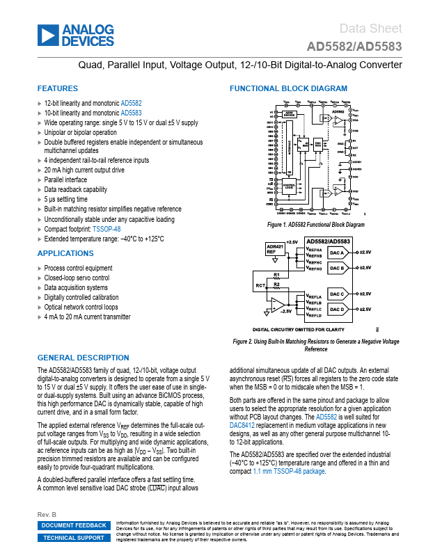
FUNCTIONAL BLOCK DIAGRAM
Figure 1. AD5582 Functional Block Diagram
GENERAL DESCRIPTION The AD5582/AD5583 family of quad, 12-/10-bit, voltage output digital-to-analog converters is designed to operate from a single 5 V to 15 V or dual ±5 V supply. It offers the user ease of use in singleor dual-supply systems. Built using an advance Bi CMOS process, this high performance DAC is dynamically stable, capable of high current drive, and in a small form factor. The applied external reference VREF determines the full-scale output voltage ranges from VSS to VDD, resulting in a wide selection of full-scale outputs. For multiplying and wide dynamic applications, ac reference inputs can be as high as |VDD
- VSS|. Two built-in precision trimmed resistors are available and can be configured easily to provide four-quadrant multiplications. A doubled-buffered parallel interface offers a fast settling time. A mon level sensitive load DAC strobe (LDAC) input allows
Figure 2. Using Built-In Matching Resistors to Generate a Negative Voltage Reference additional simultaneous update of all...