Datasheet4U Logo Datasheet4U.com

AD5696R - Quad 16-/14-/12-Bit nanoDAC+

General Description

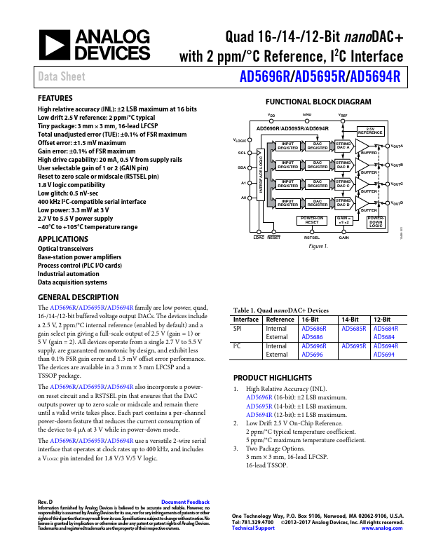
The AD5696R/AD5695R/AD5694R family are low power, quad, 16-/14-/12-bit buffered voltage output DACs.

The devices include a 2.5 V, 2 ppm/°C internal reference (enabled by default) and a gain select pin giving a full-scale output of 2.5 V (gain = 1) or 5 V (gain = 2).

Key Features

  • High relative accuracy (INL): ±2 LSB maximum at 16 bits Low drift 2.5 V reference: 2 ppm/°C typical Tiny package: 3 mm × 3 mm, 16-lead LFCSP Total unadjusted error (TUE): ±0.1% of FSR maximum Offset error: ±1.5 mV maximum Gain error: ±0.1% of FSR maximum High drive capability: 20 mA, 0.5 V from supply rails User selectable gain of 1 or 2 (GAIN pin) Reset to zero scale or midscale (RSTSEL pin) 1.8 V logic compatibility Low glitch: 0.5 nV-sec 400 kHz I2C-compatible serial interface Low power: 3.3.

📥 Download Datasheet

Full PDF Text Transcription (Reference)

The following content is an automatically extracted verbatim text from the original manufacturer datasheet and is provided for reference purposes only.

View original datasheet text
Data Sheet Quad 16-/14-/12-Bit nanoDAC+ with 2 ppm/°C Reference, I2C Interface AD5696R/AD5695R/AD5694R FEATURES High relative accuracy (INL): ±2 LSB maximum at 16 bits Low drift 2.5 V reference: 2 ppm/°C typical Tiny package: 3 mm × 3 mm, 16-lead LFCSP Total unadjusted error (TUE): ±0.1% of FSR maximum Offset error: ±1.5 mV maximum Gain error: ±0.1% of FSR maximum High drive capability: 20 mA, 0.5 V from supply rails User selectable gain of 1 or 2 (GAIN pin) Reset to zero scale or midscale (RSTSEL pin) 1.8 V logic compatibility Low glitch: 0.5 nV-sec 400 kHz I2C-compatible serial interface Low power: 3.3 mW at 3 V 2.7 V to 5.