• Part: AD5725
  • Description: Voltage Output DAC
  • Manufacturer: Analog Devices
  • Size: 484.31 KB
Download AD5725 Datasheet PDF
Analog Devices
AD5725
AD5725 is Voltage Output DAC manufactured by Analog Devices.
Data Sheet Quad, 12-Bit, Parallel Input, Unipolar/Bipolar, Voltage Output DAC Features +5 V to ±15 V operation Unipolar or bipolar operation ±0.5 LSB max INL error, ±1 LSB max DNL error Settling time: 10 µs max (10 V step) Double-buffered inputs Simultaneous updating via LDAC Asynchronous CLR to zero/mid scale Readback Operating temperature range: - 40°C to +85°C i CMOS® process technology APPLICATIONS Industrial automation Closed-loop servo control, process control Automotive test and measurement Programmable logic controllers GENERAL DESCRIPTION 
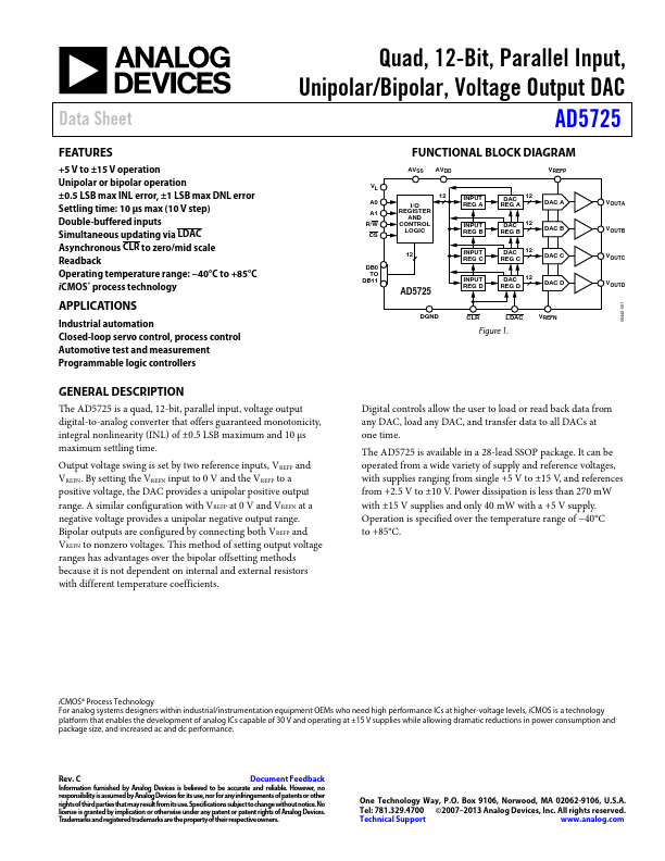
The AD5725 is a quad, 12-bit, parallel input, voltage output digital-to-analog converter that offers guaranteed monotonicity, integral nonlinearity (INL) of ±0.5 LSB maximum and 10 µs maximum settling time. Output voltage swing is set by two reference inputs, VREFP and VREFN. By setting the VREFN input to 0 V and the VREFP to a positive voltage, the DAC provides a unipolar positive output range. A similar configuration with VREFP at 0 V and VREFN at a negative voltage provides a unipolar negative output range. Bipolar outputs are configured by connecting both VREFP and VREFN to nonzero voltages. This method of setting output voltage ranges has advantages over the bipolar offsetting methods because it is not dependent on internal and external resistors with different temperature coefficients. VL A0 A1 R/W CS DB0 TO DB11 FUNCTIONAL BLOCK DIAGRAM AVSS AVDD VREFP I/O REGISTER AND CONTROL LOGIC INPUT REG A INPUT REG B INPUT REG C INPUT REG D DAC 12 REG A DAC A DAC 12 REG B DAC B DAC 12 REG C DAC C DAC 12 REG...