Analog Devices AD7002
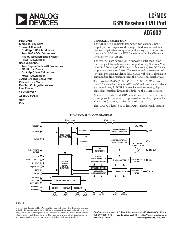
The AD7002 is a complete low power, two-channel, input/ output port with signal conditioning. The device is used as a baseband digitization subsystem, performing signal conversion between the DSP and the IF/RF sections in the Pan-European telephone system (GSM). The transmit path consists of an onboard digital modulator, containing all the code necessary for performing Gaussian Minimum Shift Keying (GMSK), two high accuracy, fast DACs with output reconstruction filters.
| Part No. |
AD7002 |
| Datasheet |
AD7002
Download
|
| Manufacturer |
 Analog Devices |
| Description |
LC2MOS GSM Baseband I/O Port |
| Buy |
Stock & Price
|
FEATURES
Single +5 V Supply Transmit Channel On-Chip GMSK Modulator Two 10-Bit D/A Converters Analog Reconstruction Filters Power-Down Mode Receive Channel Two Sigma-Delta A/D Converters FIR Digital Filters On-Chip Offset Calibration Power-Down Mode 3 Auxiliary D/A Converters Power-Down Modes On-Chip Voltage Reference Low Power 44-Lead PQFP APPLICATIONS
GSM PCN LC2MOS GSM Baseband I/O Port AD7002 GENERAL DESCRIPTION
The receive path is composed of two high performance sigma-delta ADCs with digital filtering. A common bandgap reference feeds the ADCs and signal DACs. Three control DACs (AUX DAC1 to AUX DAC3) are included for such functions as AFC, AGC and carrier signal shaping. In addition, AUX FLAG may be used for routing digital control information through the device to the IF/RF sections. As it is a necessity for all GSM mobile systems to use the lowest power possible, the device has power-down or sleep options for all sections (transmit, receive and auxiliary). The AD7002 is housed in 44-lead PQFP (Plastic Quad Flatpack).