FEATURES
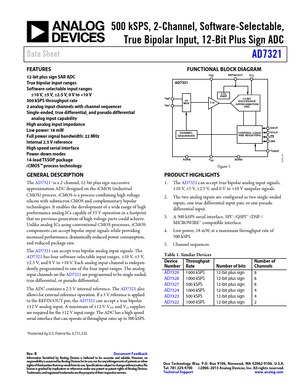
12-bit plus sign SAR ADC True bipolar input ranges Software-selectable input ranges ±10 V, ±5 V, ±2.5 V, 0 V to +10 V 500 kSPS throughput rate Two analog input channels with channel sequencer Single-ended, true differential, and pseudo differential analog input capability High analog input impedance Low power: 17 mW Full power signal bandwidth: 22 MHz Internal 2.5 V reference High speed serial interface Power-down modes 14-lead TSSOP package iCMOS™ process technology FUNCTIONAL BLOCK DIAGRAM VDD REFIN/OUT VCC AD7321 2.5V VREF I/P MUX T/H VIN0 VIN1 13-BIT SUCCESSIVE APPROXIMATION ADC DOUT CHANNEL SEQUENCER CONTROL LOGIC AND REGISTERS SCLK CS DIN VDRIVE AGND VSS DGND 05399-001 Figure 1. GENERAL DESCRIPTION
iCMOS is a process combining high voltage silicon with submicron CMOS and complementary bipolar technologies. Unlike analog ICs using conventional CMOS processes, iCMOS components can accept bipolar input signals while providing increased performance, dramatically reduced power consumption, and reduced package size. Analog Devices