FEATURES
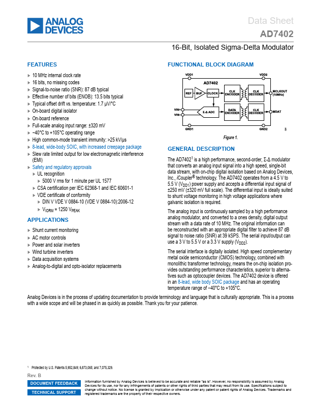
FUNCTIONAL BLOCK DIAGRAM ► 10 MHz internal clock rate ► 16 bits, no missing codes ► Signal-to-noise ratio (SNR): 87 dB typical ► Effective number of bits (ENOB): 13.5 bits typical ► Typical offset drift vs. temperature: 1.7 µV/°C ► On-board digital isolator ► On-board reference ► Full-scale analog input range: ±320 mV ► −40°C to +105°C operating range ► High common-mode transient immunity: >25 kV/µs ► 8-lead, wide-body SOIC, with increased creepage package ► Slew rate limited output for low electromagnetic interference (EMI) ► Safety and regulatory approvals ► UL recognition ► 5000 V rms for 1 minute per UL 1577 ► CSA certification per IEC 62368-1 and IEC 60601-1 ► VDE certificate of conformity ► DIN V VDE V 0884-10 (VDE V 0884-10):2006-12 ► VIORM = 1250 VPEAK APPLICATIONS
► Shunt current monitoring ► AC motor controls ► Power and solar inverters ► Wind turbine inverters ► Data acquisition systems ► Analog-to-digital and opto-isolator replacements Figure 1. GENERAL DESCRIPTION
... Analog Devices