FEATURES
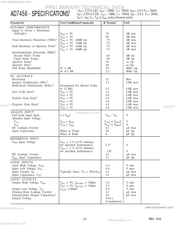
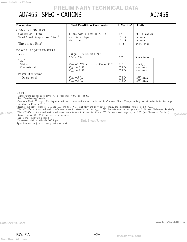
Specified for VDD of 3 V and 5 V Very Low Power: TBD mW typ at 100kSPS with 3 V Supplies TBD mW typ at 100kSPS with 5 V Supplies Fully Differential Analog Input Wide Input Bandwidth: 70dB SINAD at 20kHz Input Frequency No Pipeline Delays Serial Interface - SPI TM /QSPI TM /MICROWIRE TM / DSP Compatible Automatic Power-Down Mode 8 Pin SOT-23 and µSOIC Package APPLICATIONS
Transducer Interface Battery Powered Systems Data Acquisition Systems Portable Instrumentation Motor Control Communications Differential Input, 100kSPS, 12-Bit ADC in 8-lead SOT-23 AD7456 FUNCTIONAL BLOCK DIAGRAM VDD VIN+ VINVREF T/H 12-BIT SUCCESSIVE APPROXIMATION ADC SCLK AD7456 CONTROL LOGIC SDATA CS GND DataShee DataSheet4U.com GENERAL DESCRIPTION
The reference voltage is applied externally to the VREF pin and can be varied from 100 mV to 3.5 V depending on the power supply and what suits the application. The value of the reference voltage determines the common mode voltage range of the part. With this truly differential input structure and variable reference input, the user can select a variety of input ranges and bias points. Analog Devices