3 Specifications4
DC Specifications4 AC Specifications5 Digital Specifications 6 Switching Specifications7 Timing Specifications8 Absolute Maximum Ratings9 Thermal Characteristics9 ESD Caution 9 Pin Configuration and Function Descriptions10 Typical Performance Characteristics 11 AD9629-8011 AD9629-6
Key Features
1.8 V analog supply operation 1.8 V to 3.3 V output supply SNR
71.3 dBFS at 9.7 MHz input 69.0 dBFS at 200 MHz input SFDR 95 dBc at 9.7 MHz input 83 dBc at 200 MHz input Low power 45 mW at 20 MSPS 85 mW at 80 MSPS Differential input with 700 MHz bandwidth On-chip voltage reference and sample-and-hold circuit 2 V p-p differential analog input DNL = ±0.16 LSB Serial port control options Offset binary, gray code, or twos complement data format Integer 1, 2, or 4 input clock divider Built-in selecta.
Full PDF Text Transcription for AD9629 (Reference)
Note: Below is a high-fidelity text extraction (approx. 800 characters) for
AD9629. For precise diagrams, and layout, please refer to the original PDF.
Data Sheet 
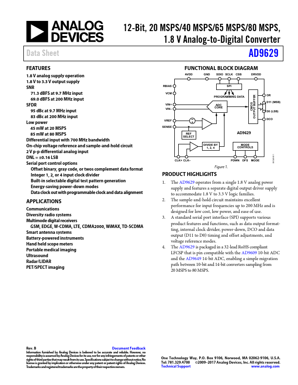
12-Bit, 20 MSPS/40 MSPS/65 MSPS/80 MSPS, 1.8 V Analog-to-Digital Converter AD9629 FEATURES 1.8 V analog supply operation 1.8 V to 3.3 V output supply SNR 71.3 ...
View more extracted text
S 1.8 V analog supply operation 1.8 V to 3.3 V output supply SNR 71.3 dBFS at 9.7 MHz input 69.0 dBFS at 200 MHz input SFDR 95 dBc at 9.7 MHz input 83 dBc at 200 MHz input Low power 45 mW at 20 MSPS 85 mW at 80 MSPS Differential input with 700 MHz bandwidth On-chip voltage reference and sample-and-hold circuit 2 V p-p differential analog input DNL = ±0.