FEATURES
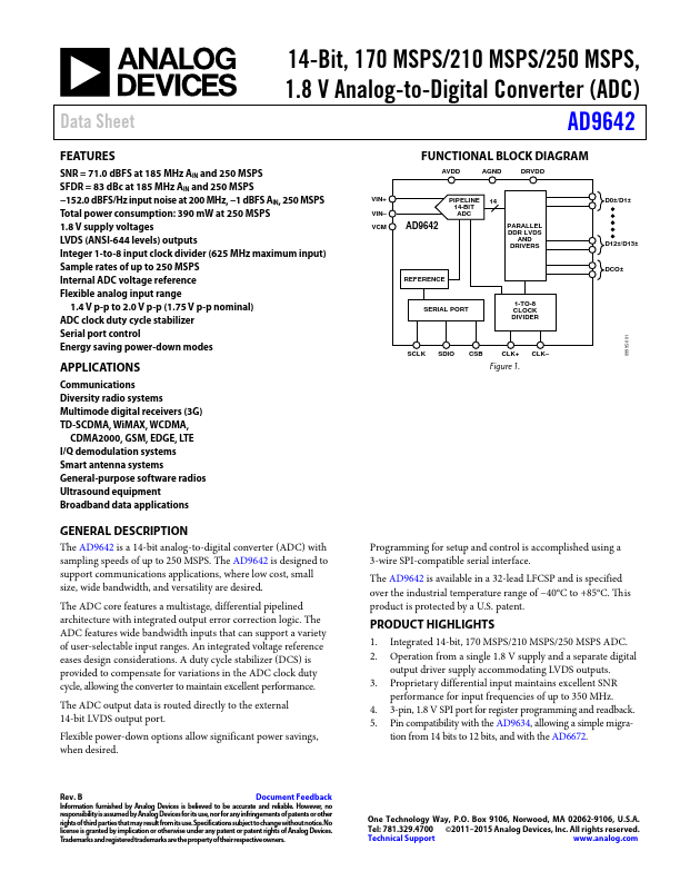
SNR = 71.0 dBFS at 185 MHz AIN and 250 MSPS SFDR = 83 dBc at 185 MHz AIN and 250 MSPS −152.0 dBFS/Hz input noise at 200 MHz, −1 dBFS AIN, 250 MSPS Total power consumption: 390 mW at 250 MSPS 1.8 V supply voltages LVDS (ANSI-644 levels) outputs Integer 1-to-8 input clock divider (625 MHz maximum input) Sample rates of up to 250 MSPS Internal ADC voltage reference Flexible analog input range 1.4 V p-p to 2.0 V p-p (1.75 V p-p nominal) ADC clock duty cycle stabilizer Serial port control Energy saving power-down modes APPLICATIONS
Communications Diversity radio systems Multimode digital receivers (3G) TD-SCDMA, WiMAX, WCDMA, CDMA2000, GSM, EDGE, LTE I/Q demodulation systems Smart antenna systems General-purpose software radios Ultrasound equipment Broadband data applications GENERAL DESCRIPTION
The ADC features wide bandwidth inputs that can support a variety of user-selectable input ranges. An integrated voltage reference eases design considerations. A duty cycle stabilizer (DCS) is provided to compensate for variations in the ADC clock duty cycle, allowing the converter to maintain excellent performance. Analog Devices