AD9708
Key Features
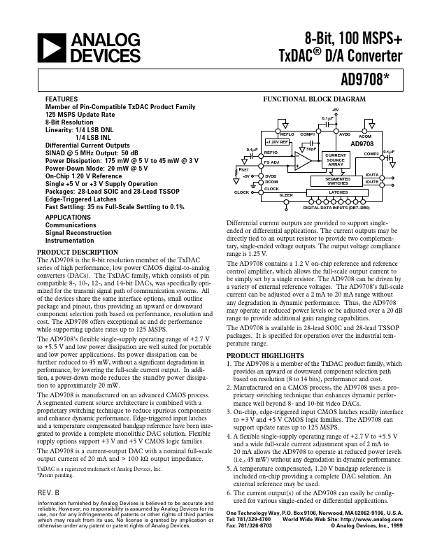
- The AD9708 is a member of the TxDAC product family, which provides an upward or downward component selection path based on resolution (8 to 14 bits), performance and cost.
- Manufactured on a CMOS process, the AD9708 uses a proprietary switching technique that enhances dynamic performance well beyond 8- and 10-bit video DACs.
- On-chip, edge-triggered input CMOS latches readily interface to +3 V and +5 V CMOS logic families. The AD9708 can support update rates up to 125 MSPS.
- A flexible single-supply operating range of +2.7 V to +5.5 V and a wide full-scale current adjustment span of 2 mA to 20 mA allows the AD9708 to operate at reduced power levels (i.e., 45 mW) without any degradation in dynamic performance.
- A temperature compensated, 1.20 V bandgap reference is included on-chip providing a complete DAC solution. An external reference may be used.
- The current output(s) of the AD9708 can easily be configured for various single-ended or differential applications. One Technology Way, P.O. Box 9106, Norwood, MA 02062-9106, U.S.A. Tel: 781/329-4700 World Wide Web Site: http://www.analog.com Fax: 781/326-8703 © Analog Devices, Inc., 1999