AD9762
AD9762 is 12-Bit/ 125 MSPS TxDAC D/A Converter manufactured by Analog Devices.
FEATURES
Member of Pin-patible Tx DAC Product Family 125 MSPS Update Rate 12-Bit Resolution Excellent Spurious Free Dynamic Range Performance SFDR to Nyquist @ 5 MHz Output: 70 d Bc Differential Current Outputs: 2 m A to 20 m A Power Dissipation: 175 m W @ 5 V to 45 m W @ 3 V Power-Down Mode: 25 m W @ 5 V On-Chip 1.20 V Reference Single +5 V or +3 V Supply Operation Package: 28-Lead SOIC and TSSOP Edge-Triggered Latches APPLICATIONS munication Transmit Channel: Basestations (Single/Multichannel Applications) ADSL/HFC Modems Direct Digital Synthesis (DDS) Instrumentation PRODUCT DESCRIPTION
0.1F
12-Bit, 125 MSPS Tx DAC® D/A Converter AD9762-
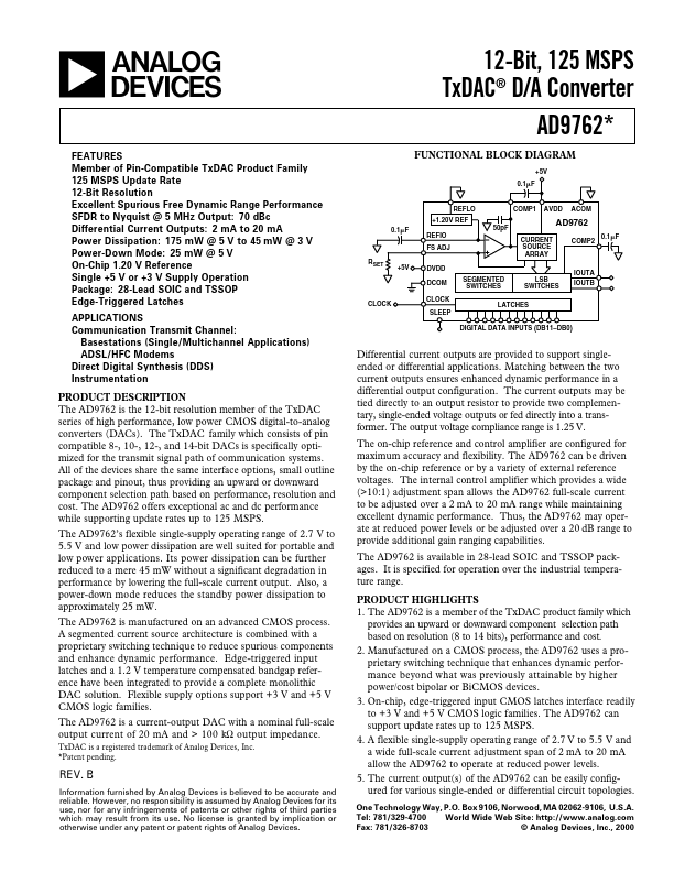
FUNCTIONAL BLOCK DIAGRAM
+5V 0.1F
REFLO +1.20V REF 50p F REFIO FS ADJ RSET +5V DVDD D CLOCK CLOCK SLEEP SEGMENTED SWITCHES
P1
AVDD
CURRENT SOURCE ARRAY P2 0.1F
IOUTA LSB SWITCHES IOUTB
LATCHES
DIGITAL DATA INPUTS (DB11- DB0)
The AD9762 is the 12-bit resolution member of the Tx DAC series of high performance, low power CMOS digital-to-analog converters (DACs). The Tx DAC family which consists of pin patible 8-, 10-, 12-, and 14-bit DACs is specifically optimized for the transmit signal path of munication systems. All of the devices share the same interface options, small outline package and pinout, thus providing an upward or downward ponent selection path based on performance, resolution and cost. The AD9762 offers exceptional ac and dc performance while supporting update rates up to 125 MSPS. The AD9762’s flexible single-supply operating range of 2.7 V to 5.5 V and low power dissipation are well suited for portable and low power applications. Its power dissipation can be further reduced to a mere 45 m W without a significant degradation in performance by lowering the full-scale current output. Also, a power-down mode reduces the standby power dissipation to approximately 25 m W. The AD9762 is manufactured on an advanced CMOS process. A segmented current source architecture is bined with a proprietary switching technique...