AD9834
AD9834 is 75 MHz Complete DDS manufactured by Analog Devices.
Data Sheet
20 mW Power, 2.3 V to 5.5 V, 75 MHz plete DDS AD9834
Features
Narrow-band SFDR >72 dB 2.3 V to 5.5 V power supply Output frequency up to 37.5 MHz Sine output/triangular output On-board parator 3-wire SPI® interface
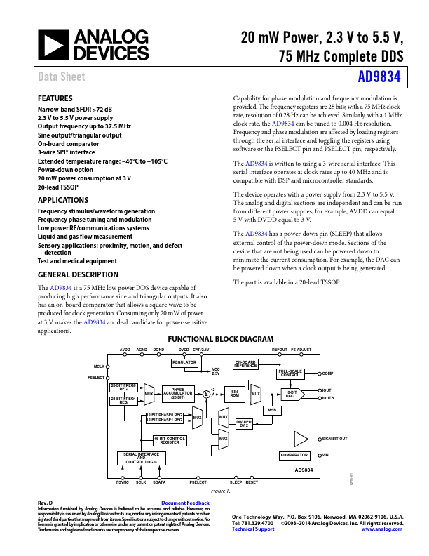
Capability for phase modulation and frequency modulation is provided. The frequency registers are 28 bits; with a 75 MHz clock rate, resolution of 0.28 Hz can be achieved. Similarly, with a 1 MHz clock rate, the AD9834 can be tuned to 0.004 Hz resolution. Frequency and phase modulation are affected by loading registers through the serial interface and toggling the registers using software or the FSELECT pin and PSELECT pin, respectively.
Extended temperature...