Datasheet4U Logo Datasheet4U.com

ADCLK854 - Low Power Clock Fanout Buffer

Description

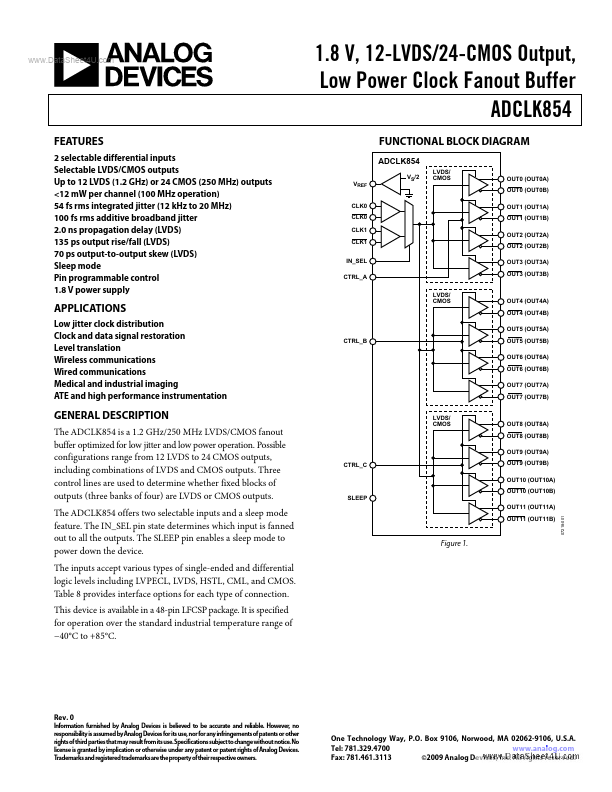
The ADCLK854 is a 1.2 GHz/250 MHz LVDS/CMOS fanout buffer optimized for low jitter and low power operation.

Possible configurations range from 12 LVDS to 24 CMOS outputs, including combinations of LVDS and CMOS outputs.

Features

  • 2 selectable differential inputs Selectable LVDS/CMOS outputs Up to 12 LVDS (1.2 GHz) or 24 CMOS (250 MHz) outputs.

📥 Download Datasheet

Datasheet preview – ADCLK854

Datasheet Details

Part number ADCLK854
Manufacturer Analog Devices
File Size 724.65 KB
Description Low Power Clock Fanout Buffer
Datasheet download datasheet ADCLK854 Datasheet
Additional preview pages of the ADCLK854 datasheet.
Other Datasheets by Analog Devices

Full PDF Text Transcription

Click to expand full text
www.DataSheet4U.com 1.8 V, 12-LVDS/24-CMOS Output, Low Power Clock Fanout Buffer ADCLK854 FUNCTIONAL BLOCK DIAGRAM ADCLK854 VREF CLK0 CLK0 CLK1 CLK1 IN_SEL CTRL_A LVDS/ CMOS VS/2 LVDS/ CMOS OUT0 (OUT0A) OUT0 (OUT0B) OUT1 (OUT1A) OUT1 (OUT1B) OUT2 (OUT2A) OUT2 (OUT2B) OUT3 (OUT3A) OUT3 (OUT3B) FEATURES 2 selectable differential inputs Selectable LVDS/CMOS outputs Up to 12 LVDS (1.2 GHz) or 24 CMOS (250 MHz) outputs <12 mW per channel (100 MHz operation) 54 fs rms integrated jitter (12 kHz to 20 MHz) 100 fs rms additive broadband jitter 2.0 ns propagation delay (LVDS) 135 ps output rise/fall (LVDS) 70 ps output-to-output skew (LVDS) Sleep mode Pin programmable control 1.
Published: |