Datasheet4U Logo Datasheet4U.com

ADCMP562 - (ADCMP561 / ADCMP562) Dual High Speed PECL Comparators

Download the ADCMP562 datasheet PDF. This datasheet also covers the ADCMP561 variant, as both devices belong to the same (adcmp561 / adcmp562) dual high speed pecl comparators family and are provided as variant models within a single manufacturer datasheet.

General Description

The ADCMP561/ADCMP562 are high speed comparators fabricated on Analog Devices’ proprietary XFCB process.

The devices feature a 700 ps propagation delay with less than 75 ps overdrive dispersion.

Key Features

  • Differential PECL compatible outputs 700 ps propagation delay input to output 75 ps propagation delay dispersion Input common-mode range:.
  • 2.0 V to +3.0 V Robust input protection Differential latch control Internal latch pull-up resistors Power supply rejection greater than 85 dB 700 ps minimum pulse width 1.5 GHz equivalent input rise time bandwidth Typical output rise/fall time of 500 ps ESD protection > 4kV HBM, >200V MM Programmable hysteresis.

📥 Download Datasheet

Note: The manufacturer provides a single datasheet file (ADCMP561_AnalogDevices.pdf) that lists specifications for multiple related part numbers.

Datasheet Details

Part number ADCMP562
Manufacturer Analog Devices
File Size 335.06 KB
Description (ADCMP561 / ADCMP562) Dual High Speed PECL Comparators
Datasheet download datasheet ADCMP562 Datasheet

Full PDF Text Transcription (Reference)

The following content is an automatically extracted verbatim text from the original manufacturer datasheet and is provided for reference purposes only.

View original datasheet text
Dual High Speed PECL Comparators ADCMP561/ADCMP562 FEATURES Differential PECL compatible outputs 700 ps propagation delay input to output 75 ps propagation delay dispersion Input common-mode range: –2.0 V to +3.0 V Robust input protection Differential latch control Internal latch pull-up resistors Power supply rejection greater than 85 dB 700 ps minimum pulse width 1.5 GHz equivalent input rise time bandwidth Typical output rise/fall time of 500 ps ESD protection > 4kV HBM, >200V MM Programmable hysteresis 
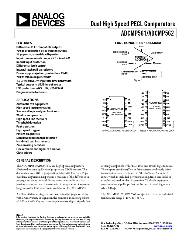
FUNCTIONAL BLOCK DIAGRAM HYS* NONINVERTING INPUT Q OUTPUT ADCMP561/ ADCMP562 INVERTING INPUT Q OUTPUT *ADCMP562 ONLY Figure 1.